

Plasma measuring method, plasma measuring device and storage medium
a plasma and measuring device technology, applied in the field of plasma measuring methods, can solve the problems of complex operation, multiple operation, and difficult positioning of plasma absorption probes, and achieve the effect of convenient optimization and high efficiency
Inactive Publication Date: 2010-12-23
TOKYO ELECTRON LTD
View PDF4 Cites 8 Cited by
- Summary
- Abstract
- Description
- Claims
- Application Information
AI Technical Summary
Benefits of technology
The present invention relates to improving semiconductor device manufacturing by controlling the distribution of electrons during plasma processing. By measuring both the electric current (etching rate) and the number of electrons, this technology allows for easy optimization of process settings that result in optimal performance. This helps improve efficiency and accuracy in developing new processes while reducing costs associated with trial-and-error methods.
Problems solved by technology
The technical problem addressed in this patent text is the need to improve in-plane uniformity of semiconductor device manufacturing processes using plasma techniques. The process conditions affect the plasma generated in the processing chamber, and changes in parameters of these conditions lead to changes in electron density distribution and etching rate distribution. However, it is difficult to determine whether an electrically negative or positive plasma is generated under certain process conditions, and no determining method is established. This makes it difficult to optimize the process conditions and achieve high in-plane uniformity of the electron density distribution or etching rate distribution.
Method used
View moreImage
Smart ImageViewing Examples

Examples
 PUM
 Abstract
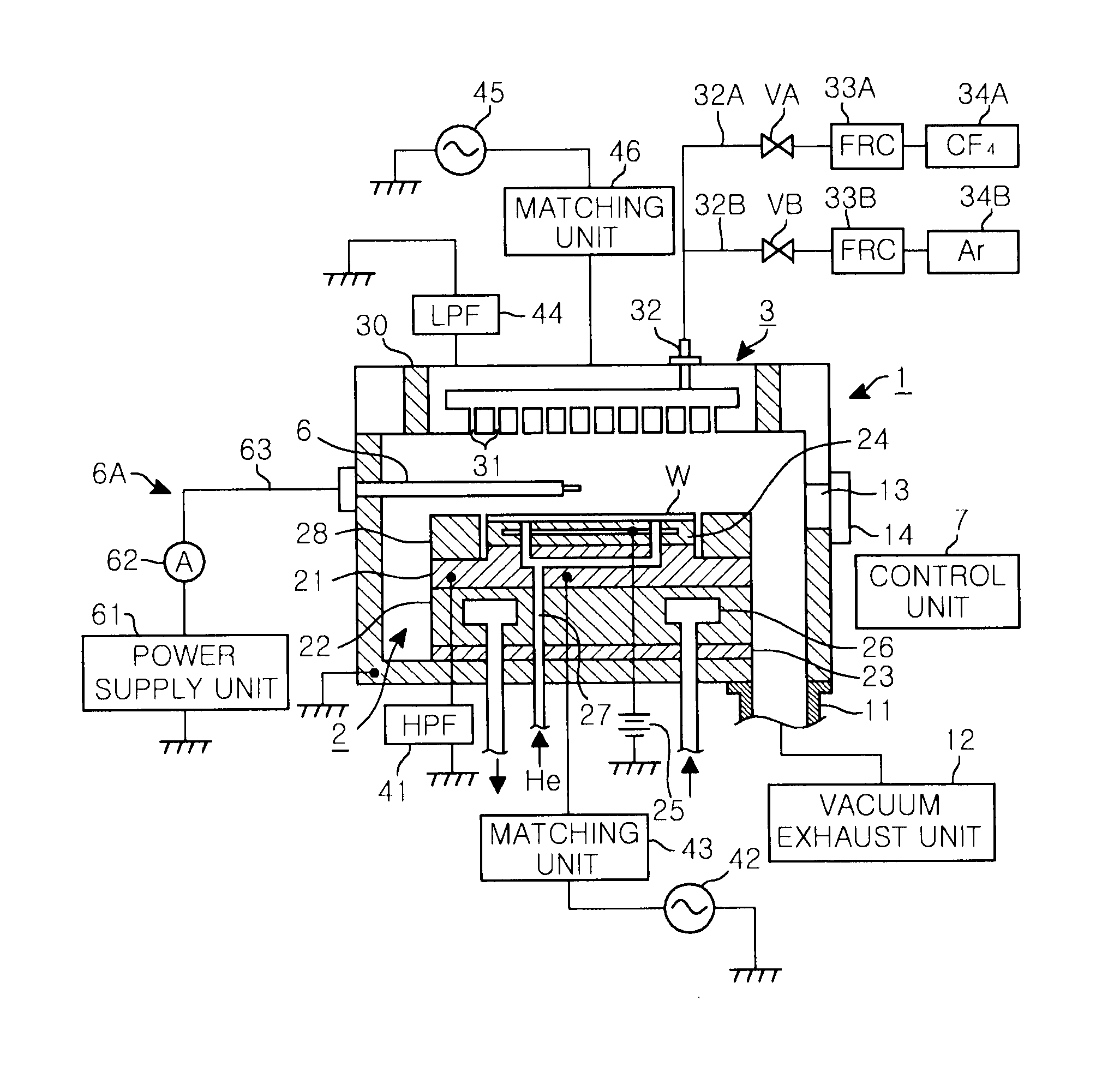
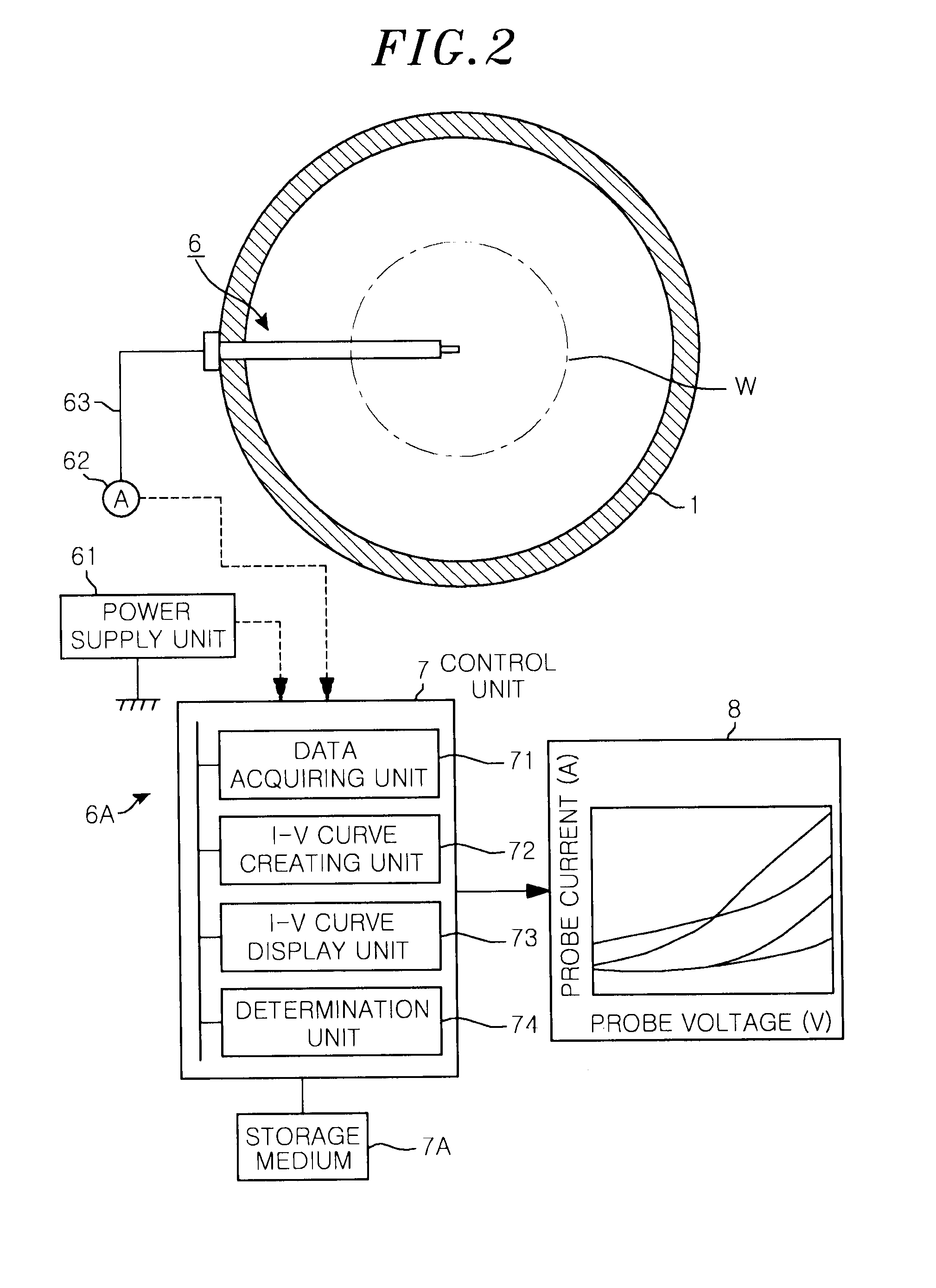
Provided is a technique capable of ascertaining the process condition of the boundary between electrically positive and negative plasma regions. In a vacuum chamber, one of the parameters of process conditions is stepwisely changed to generate a plasma under at least three process conditions. The parameters include a flow rate ratio between an electrically negative gas and an electrically positive gas, a pressure in the vacuum chamber and the magnitude of an energy supplied to the gases. Next, a voltage is applied to a Langmuir probe positioned in that plasma, and a current-voltage curve indicating the relationship between the applied voltage and the electric current to flow through the probe is acquired for each of the process conditions. On the basis of the current-voltage curve group acquired, the process conditions are determined for the boundary between the electrically positive and negative plasma regions.
Description
Login to View More Claims
Login to View More Application Information
Patent Timeline
 OwnerTOKYO ELECTRON LTD