
Three-dimensional integrated circuit structure

Inactive Publication Date: 2011-01-06
LEE SANG YUN
View PDF11 Cites 206 Cited by
  • Summary
  • Abstract
  • Description
  • Claims
  • Application Information

AI Technical Summary

Problems solved by technology

However, these laterally oriented devices consume significant amounts of chip area.
However, the 64-bit computer chip will need more devices since there are more bits to process at a given time.
The number of devices can be increased by making the devices included therein smaller, but this requires advances in lithography and increasingly expensive manufacturing equipment.
However, the yield of the computer chips fabricated in a run decreases as their area increases, which increases the overall cost.
However, there are several problems with this.
One problem is that the masks used to fabricate the memory devices are not necessarily compatible with the masks used to fabricate the other electronic devices.
Hence, it is more complex and expensive to fabricate a computer chip with memory embedded in this way.
Another problem is that memory devices tend to be large and occupy a significant amount of area.
The total area of the computer chip can be increased, but as discussed above, this decreases the yield and increases the cost.

Method used


Image

  • Three-dimensional integrated circuit structure
  • Three-dimensional integrated circuit structure
  • Three-dimensional integrated circuit structure

Examples


Embodiment Construction

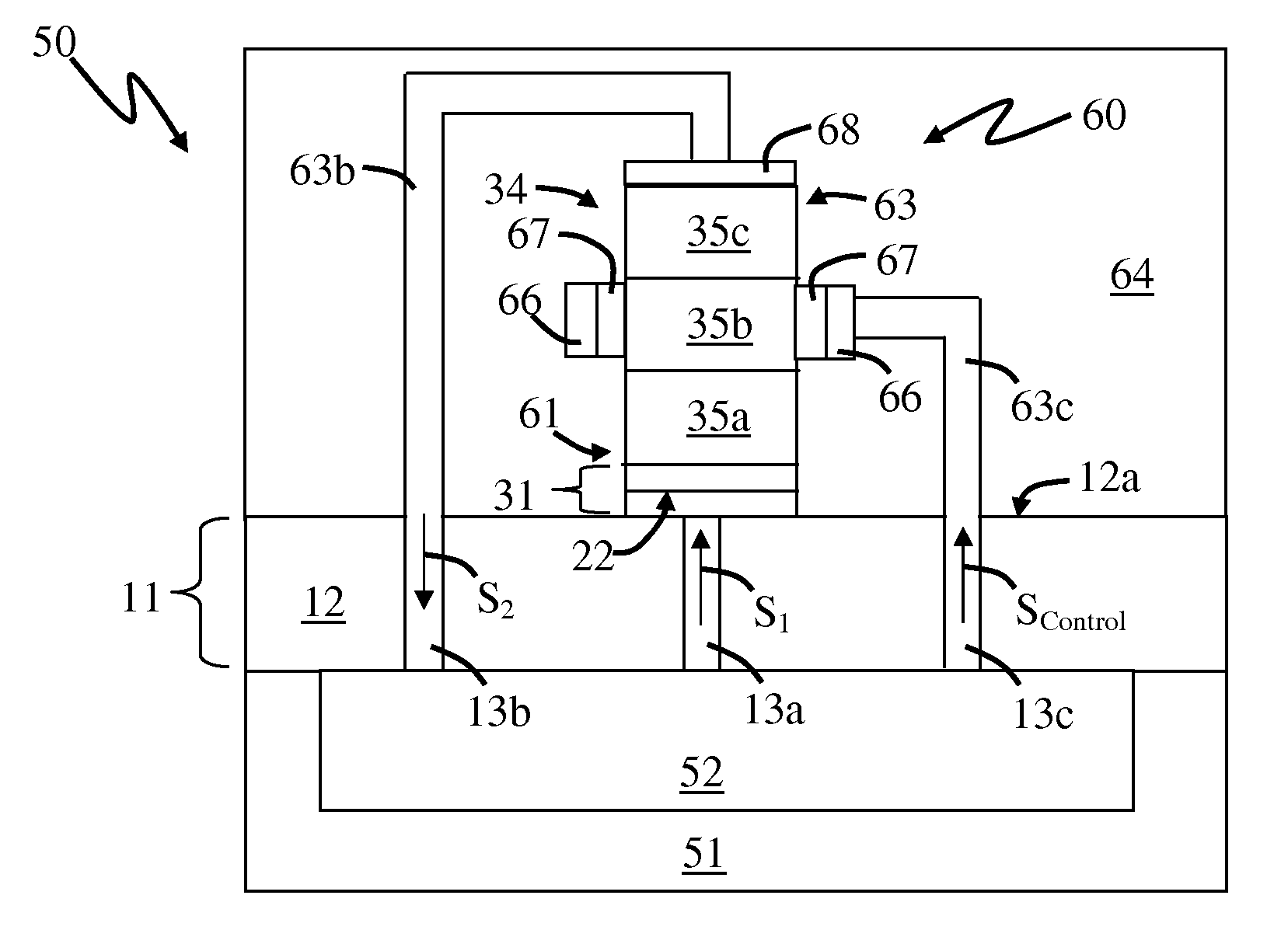
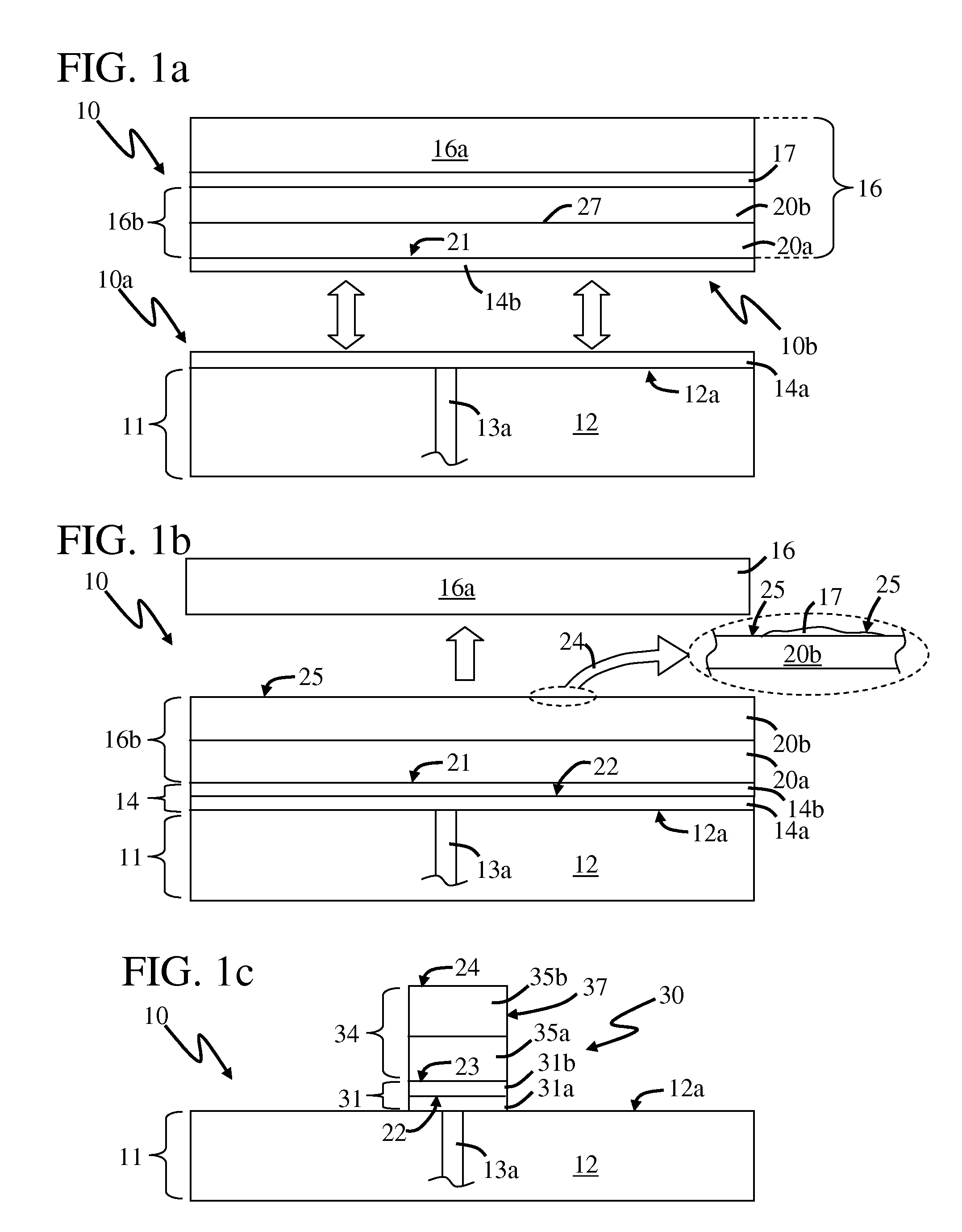
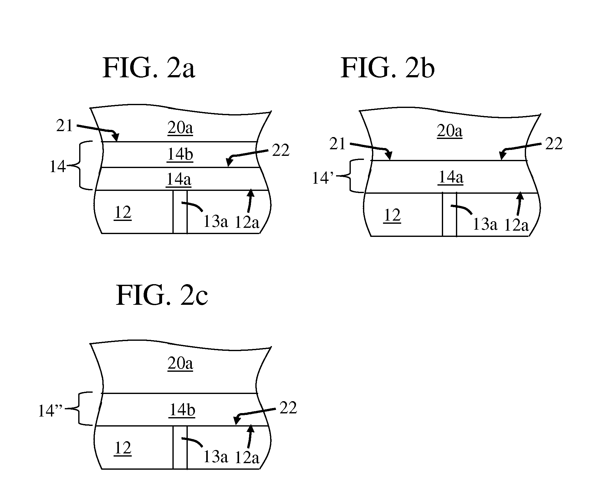
[0035]A semiconductor structure is disclosed for use with an electronic circuit in a computer chip. The semiconductor structure is bonded to an interconnect region and processed to form one or more vertically oriented semiconductor devices which are positioned above the electronic circuit. One or more of the vertically oriented semiconductor devices are in communication with the electronic circuit through a corresponding conductive line of the interconnect region. A vertically oriented semiconductor device is in communication with the electronic circuit through the corresponding conductive line because a signal can flow between the vertically oriented semiconductor device and electronic circuit through the conductive line. The signal flows between the vertically oriented semiconductor device and electronic circuit through the conductive line so that the electronic circuit can control the operation of the vertically oriented semiconductor device. It should be noted that vertically or...


PUM


Abstract

A semiconductor structure includes an interconnect region and a semiconductor stack bonded to the interconnect region through a bonding region. The stack includes two semiconductor layers having different electrical properties. The stack also includes single crystalline semiconductor material. The stack can be processed to form a mesa structure and the mesa structure can be processed to from a vertically oriented semiconductor device.

Description

CROSS-REFERENCE TO RELATED APPLICATIONS[0001]This application is a continuation-in-part of, and claims the benefit of, U.S. patent application Ser. Nos.:[0002]11 / 092,500, filed on Mar. 29, 2005;[0003]11 / 092,501, filed on Mar. 29, 2005;[0004]11 / 180,286, filed on Jul. 12, 2005;[0005]11 / 378,059, filed on Mar. 17, 2006;[0006]11 / 606,523, filed on Nov. 30, 2006;[0007]11 / 873,719, filed on Oct. 17, 2007;[0008]11 / 873,769, filed on Oct. 17, 2007;[0009]12 / 040,642, filed on Feb. 29, 2008;[0010]12 / 165,475, filed on Jun. 30, 2008;[0011]12 / 397,309, filed Mar. 3, 2009;[0012]12 / 470,344, filed on May 21, 2009;[0013]12 / 475,294, filed on May 29, 2009;[0014]12 / 581,722, filed on Oct. 19, 2009;[0015]12 / 618,542, filed on Nov. 13, 2009;[0016]12 / 635,496, filed on Dec. 10, 2009;[0017]12 / 637,559, filed on Dec. 14, 2009;[0018]12 / 731,087, filed on Mar. 24, 2010;[0019]12 / 847,374, filed on Jul. 30, 2010; and[0020]12 / 874,866, filed on Sep. 2, 2010,by the same inventor, the contents of all of these applications are ...

Claims


Application Information

Patent Timeline
IPC IPC(8): H01L29/78H01L23/52
CPCH01L21/2007H01L21/76254H01L2924/1301H01L21/823431H01L21/823487H01L23/52H01L24/83H01L2224/291H01L2224/8385H01L2924/0101H01L2924/01013H01L2924/01015H01L2924/01018H01L2924/01029H01L2924/01042H01L2924/01047H01L2924/01049H01L2924/01073H01L2924/01074H01L2924/01078H01L2924/01079H01L2924/07802H01L2924/13091H01L2924/14H01L2924/19041H01L2924/19042H01L2924/19043H01L24/29H01L2924/01006H01L2924/01033H01L27/1052H01L2924/00H01L2924/12036H10B99/00
Inventor LEE, SANG-YUN
Owner LEE SANG YUN
Features
  • Generate Ideas
  • Intellectual Property
  • Life Sciences
  • Materials
  • Tech Scout
  • Unparalleled Data Quality
  • Higher Quality Content
  • 60% Fewer Hallucinations
Learn More