Assembly of a wire element with a microelectronic chip with a groove comprising at least one bump securing the wire element

a microelectronic chip and groove technology, applied in the direction of basic electric elements, solid-state devices, electric apparatus, etc., can solve the problems of increasing the force to be applied when embedding, difficult to perform embedding without damaging the chip, and unsuitable for flexible structure integration

Active Publication Date: 2011-01-06
COMMISSARIAT A LENERGIE ATOMIQUE ET AUX ENERGIES ALTERNATIVES
View PDF17 Cites 81 Cited by
  • Summary
  • Abstract
  • Description
  • Claims
  • Application Information

AI Technical Summary

Benefits of technology

[0004]The object of the invention is to produce a chip having a groove designed to accommodate a wire element by embedding, limiting the forces exerted on the wire when the latter is inserted in the groove.

Problems solved by technology

However, this approach has the major drawback of using a rigid mechanical support, which is particularly unsuitable for integration in flexible structures.
Furthermore, depending on the length of groove 4, the forces to be applied when embedding is performed increase, thus making it difficult to perform embedding without damaging the chip.

Method used


Image

  • Assembly of a wire element with a microelectronic chip with a groove comprising at least one bump securing the wire element
  • Assembly of a wire element with a microelectronic chip with a groove comprising at least one bump securing the wire element
  • Assembly of a wire element with a microelectronic chip with a groove comprising at least one bump securing the wire element

Examples


Embodiment Construction

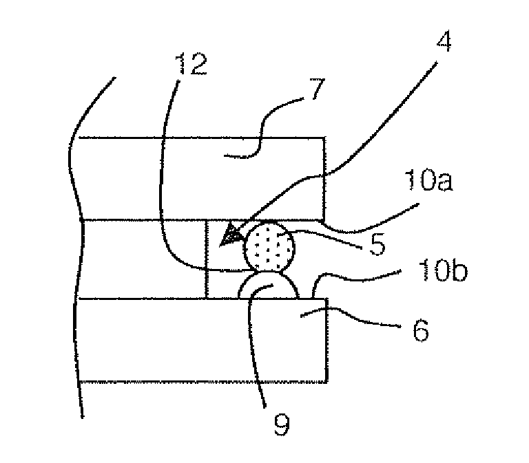
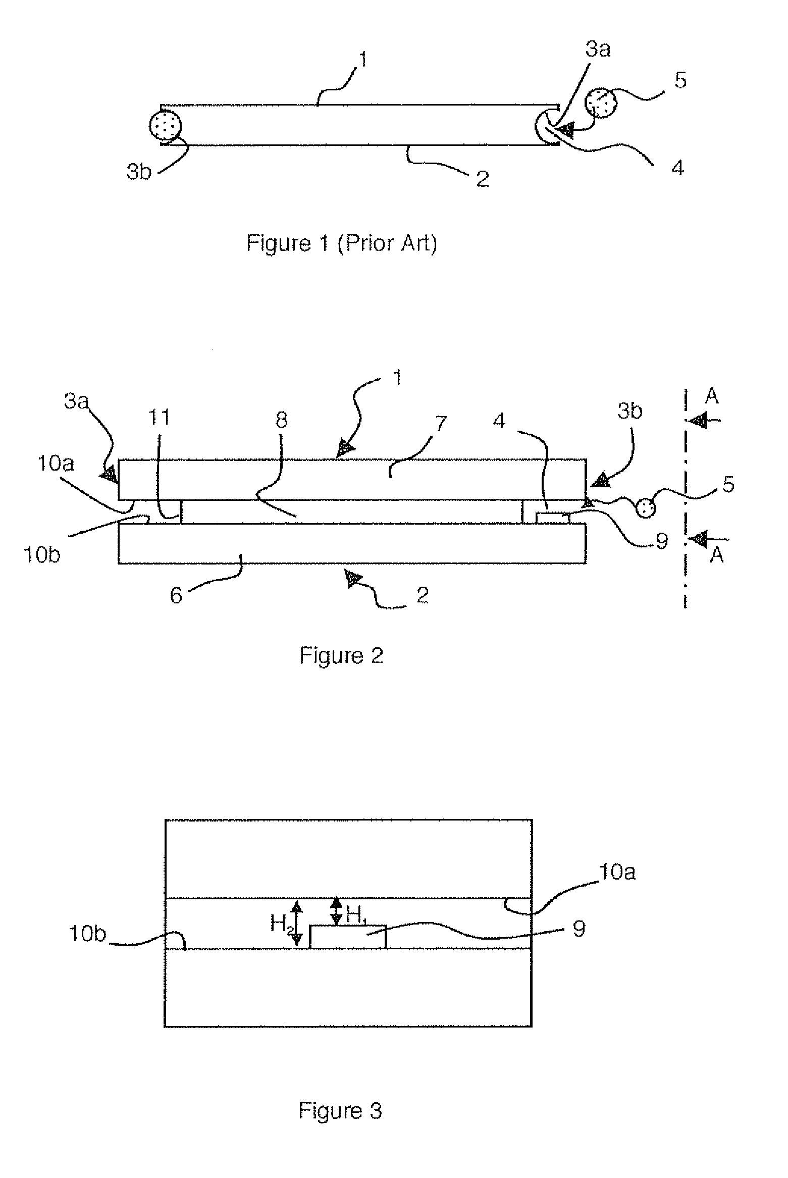
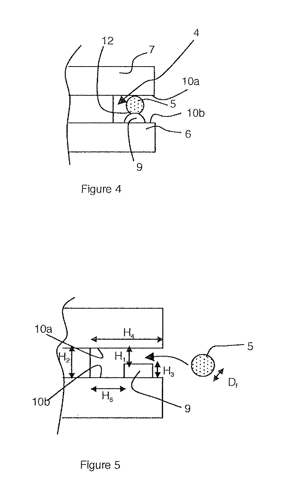
[0017]As illustrated in FIG. 2, a microelectronic chip according to the invention comprises two parallel main surfaces 1, 2 and lateral surfaces 3a and 3b. At least one of lateral surfaces 3a, 3b comprises a longitudinal groove 4. Groove 4 is delineated by two side walls 10a and 10b and a bottom 11. The groove is designed to accommodate a wire element having a longitudinal axis that is parallel to the longitudinal axis of the groove.

[0018]This type of chip can be in the form of an assembly of two microelectronic components or of a microelectronic component 6 and a counter-plate 7, of substantially the same dimensions and joined to one another by a spacer 8. The spacer being of smaller dimensions than those of the component, placement thereof enables at least one groove 4 to be obtained naturally. As illustrated in FIG. 2, the chip can comprise two grooves 4 arranged on each side of spacer 8. Grooves 4 are thus obtained by assembly of the chip, avoiding a complex machining step that ...


PUM

PropertyMeasurementUnit
height H3aaaaaaaaaa
height H3aaaaaaaaaa
height H3aaaaaaaaaa

Abstract

The assembly comprises at least one microelectronic chip having two parallel main surfaces and lateral surfaces, at least one of the lateral faces comprising a longitudinal groove housing a wire element having an axis parallel to the longitudinal axis of the groove. The groove is delineated by at least two side walls. The wire element is secured to the chip at the level of a clamping area between at least one bump arranged on one of the side walls, and the side wall of the groove opposite said bump. The clamping area has a smaller height than the diameter of the wire element and a free area is arranged laterally to the bump along the longitudinal axis of the groove. The free area has a height, corresponding to the distance separating the two side walls, that is greater than the diameter of the wire element.

Description

BACKGROUND OF THE INVENTION[0001]The invention relates to an assembly comprising at least one microelectronic chip provided with two parallel main surfaces and with lateral surfaces, at least one of the lateral surfaces comprising a longitudinal groove for housing a wire element having an axis parallel to the longitudinal axis of the groove, said groove being delineated by at least two side walls.STATE OF THE ART[0002]Numerous techniques for mechanically and electrically connecting microelectronic chips to one another exist at the present time. The conventional technique consists in making a rigid mechanical connection between the chips, once the chips have been formed on a substrate and released by dicing. The chips, fixed onto a rigid support, are then electrically connected before a protective coating is formed. This first approach, consisting in making a connection on a rigid support, is conventionally used when a great complexity in connection of the chips exists. However, this...

Claims


Application Information

Patent Timeline
Patent Type & Authority Applications(United States)
IPC IPC(8): H01L23/498
CPCH01L2924/20758H01L2924/01082H01L24/78H01L2924/01029H01L2924/01033H01L2924/20757H01L2924/20759Y10T29/41H01L2924/01028H01L24/85H01L2224/78301H01L2924/20753H01L21/6835H01L2924/01013H01L2924/01004H01L2924/01005H01L25/0655H01L2924/01006H01L2924/01014H01L24/48H01L2924/20751H01L2224/451H01L2224/85001H01L2924/014H01L2924/20756H01L2223/6677H01L2224/85365H01L25/50H01L2924/10253H01L2924/00014H01L2224/45015H01L2924/20755H01L2224/48H01L2924/01074H01L2924/01058H01L2924/01047H01L2924/2076H01L2924/01075H01L2924/01079H01L2924/20754H01L2924/20752H01L2924/00H01L2224/45139H01L2224/45144H01L24/45H01L2924/00011H01L2224/85399H01L2224/05599
Inventor BRUN, JEANVICARD, DOMINIQUEVERRUN, SOPHIE
Owner COMMISSARIAT A LENERGIE ATOMIQUE ET AUX ENERGIES ALTERNATIVES
Why Eureka
Try Eureka