Image sensor package structure with large air cavity

a technology of image sensor and package structure, which is applied in the direction of basic electric elements, electrical appliances, semiconductor devices, etc., can solve the problems of poor imaging quality, ghost images, and short distance between the transparent lid and the image sensor chip, so as to improve the imaging quality of the image sensor package structure, simplify the manufacturing process, and increase the distance between the transparent lid and the chip.

Active Publication Date: 2011-02-03
TONG HSING ELECTRONICS IND LTD
View PDF3 Cites 29 Cited by
  • Summary
  • Abstract
  • Description
  • Claims
  • Application Information

AI Technical Summary

Benefits of technology

[0012]1. By enlarging the air cavity in volume and increasing the distance between the transparent lid and the chip, the improved imaging quality of the image sensor package structure can be achieved.
[0013]2. Since the transparent lid and the plastic sheet are combined by means of injection molding, the manufacturing process can be simplified and the manufacturing cost can be therefore reduced.
[0014]3. By covering the periphery of the upper surface of the transparent lid with the package material, the blockage area from moisture to the chip is extended, thereby ensuring the image-sensing effect of the image sensor package structure against moisture.

Problems solved by technology

Traditionally in downsizing an image sensor, it is the general approach to adhere the transparent lid right on top of the image sensor chip, resulting in a very short distance between the transparent lid and the image sensor chip.
As a result, when light passes through the transparent lid and enters into the sensitization area of the image sensor chip, the multi-refraction or multi-reflection of light is likely to occur, leading to poor imaging quality as well as ghost images.

Method used


Image

  • Image sensor package structure with large air cavity
  • Image sensor package structure with large air cavity
  • Image sensor package structure with large air cavity

Examples


Embodiment Construction

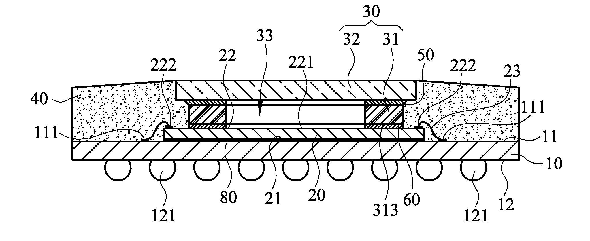
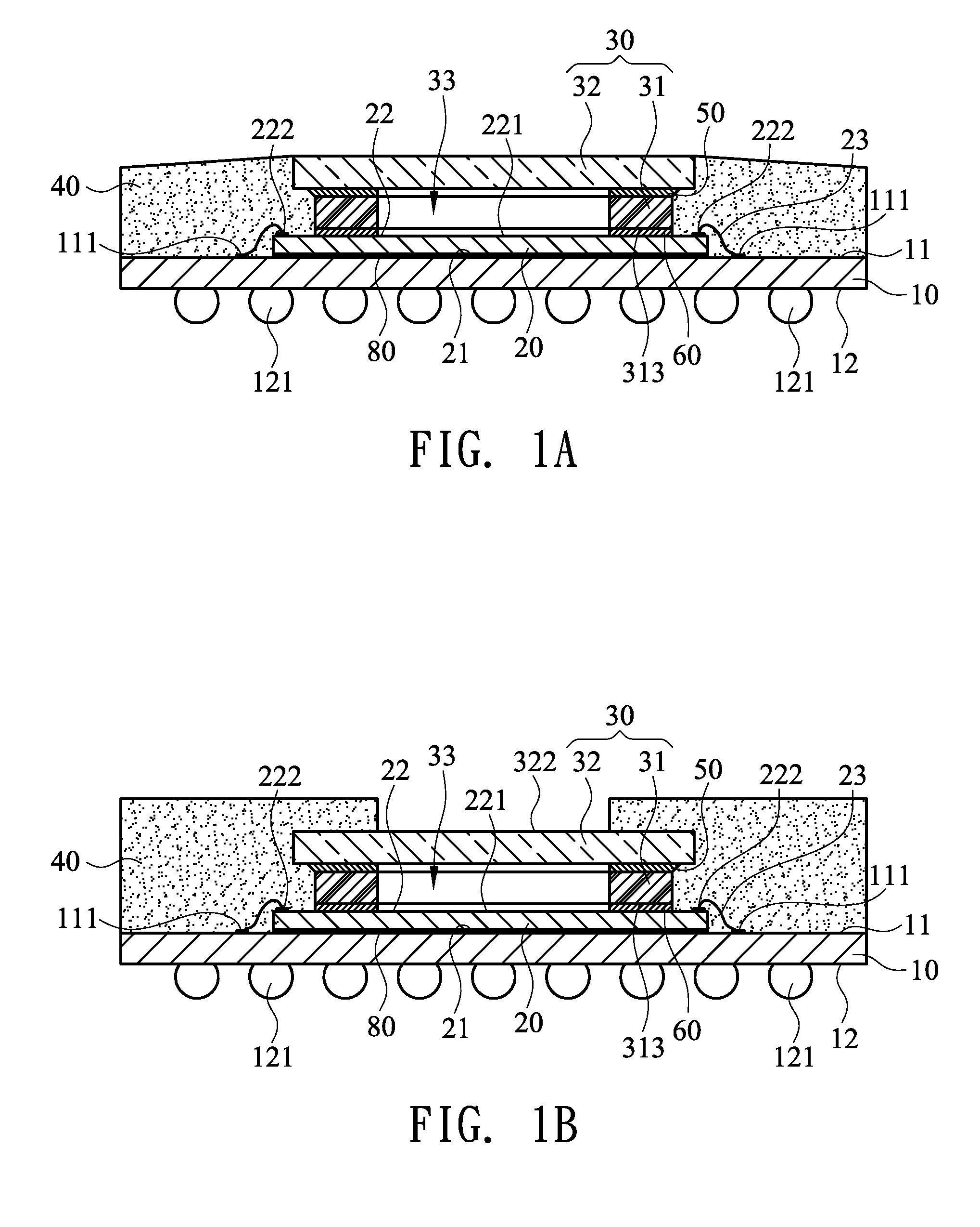
[0028]Please refer to FIG. 1A for an image sensor package structure with a large air cavity according to a first embodiment of the present invention. The image sensor package structure includes a substrate 10, a chip 20, a cover 30, and a package material 40.

[0029]As shown in FIG. 1A, the substrate 10 is one normally used in existing image sensor package structures, such as a circuit substrate. The substrate 10 has a first surface 11 and a second surface 12. Therein, the first surface 11 is an upper surface of the substrate 10 while the second surface 12 is a lower surface of the substrate 10. The first surface 11 of the substrate 10 is provided with a plurality of first conductive contacts 111 and the second surface 12 is arranged with a plurality of solder balls 121. By virtue of a circuit structure contained in the substrate 10, the first conductive contacts 111 and the solder balls 121 are electrically connected, so that the image sensor package structure can be further electric...


PUM


Abstract

The present invention discloses an image sensor package structure with a large air cavity. The image sensor package structure includes a substrate, a chip, a cover and a package material. The chip is combined with the substrate. A plastic sheet of the cover is adhered to the chip and a transparent lid of the cover is combined with the plastic sheet to provide a covering over a sensitization area of the chip so as to form an air cavity. The package material is arranged on the substrate and encapsulated around the chip and the cover. The plastic sheet having a predetermined thickness can increase the distance between the transparent lid and the chip to enlarge the air cavity. Thus, the image-sensing effect of the image sensor package structure can be improved and the ghost image problem resulting from multi-refraction and multi-reflection of light can be minimized.

Description

BACKGROUND OF THE INVENTION[0001]1. Technical Field[0002]The present invention relates to image sensor package structures. More particularly, the present invention relates to an image sensor package structure with a large air cavity, wherein the image sensor package structure provides an improved image-sensing effect.[0003]2. Description of Related Art[0004]With the ongoing progress of technology, all manufacturers of electronic multimedia devices have made every effort to improve functionality and performance of their products with the attempt to meet all the consumer demands related to audio and / or video entertainments. In such popular electronic multimedia devices, image sensors play a critical role. An image sensor serves to receive and convert optical signals into electrical signals, and transmit the electrical signals to an external device that analyzes the electrical signals. When incorporated in an electronic device, the image sensor enables the electronic device to take sti...

Claims


Application Information

Patent Timeline
Patent Type & Authority Applications(United States)
IPC IPC(8): H01L31/0203
CPCH01L27/14618H01L27/14683H01L2224/48091H01L2224/48227H01L2224/32225H01L2924/15311H01L2924/16235H01L2924/1815H01L2924/3025H01L2224/73265H01L2924/00014H01L2224/45099H01L2924/00H01L2924/00012H01L24/73H01L2924/181H01L2224/73215
Inventor TU, HSIU-WENKUO, REN-LONGSHIAO, YOUNG-HOUNGCHEN, TSAO-PINHO, MON-NAMHSU, CHIH-CHENGLIN, CHIN-FUHSIN, CHUNG-HSIEN
Owner TONG HSING ELECTRONICS IND LTD
Why Eureka
Try Eureka