
Mechanical Barrier Element for Improved Thermal Reliability of Electronic Components

a technology of electronic components and barrier elements, which is applied in the direction of semiconductor devices, semiconductor/solid-state device details, electrical devices, etc., can solve the problems of increasing the difficulty of providing efficient heat dissipation mechanisms, damage to delicate and tiny structures,

Inactive Publication Date: 2011-02-24
GLOBALFOUNDRIES INC
View PDF4 Cites 26 Cited by
  • Summary
  • Abstract
  • Description
  • Claims
  • Application Information

AI Technical Summary

Benefits of technology

[0006]The present invention is generally related to packaging of integrated circuit devices, and more s

Problems solved by technology

Heat can damage the delicate and tiny structures which allow transistors to function as intended in a semiconductor device.
As semiconductor devices become smaller and smaller, it has become more difficult to provide efficient heat dissipation mechanisms.

Method used


Image

  • Mechanical Barrier Element for Improved Thermal Reliability of Electronic Components
  • Mechanical Barrier Element for Improved Thermal Reliability of Electronic Components
  • Mechanical Barrier Element for Improved Thermal Reliability of Electronic Components

Examples


Embodiment Construction

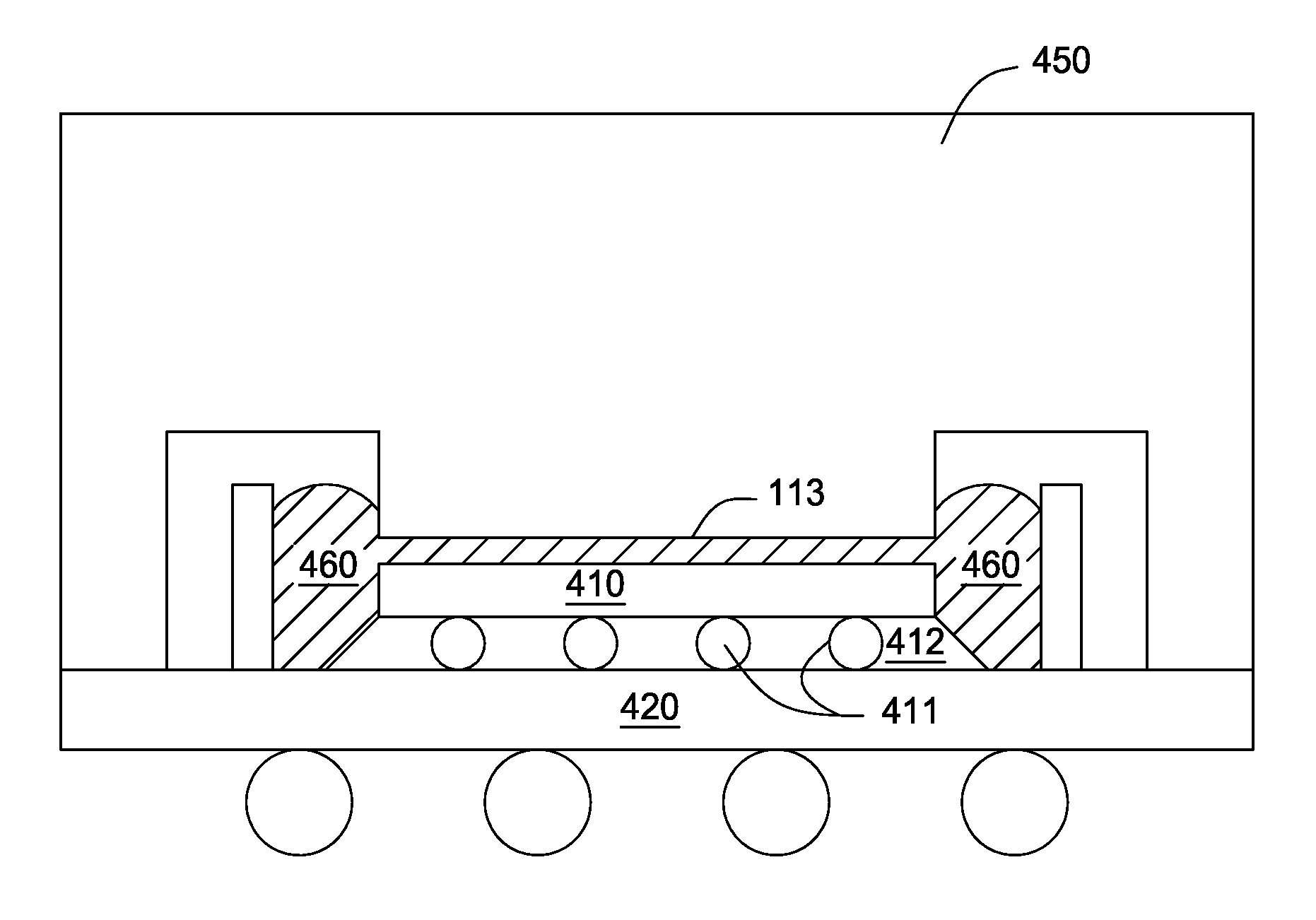
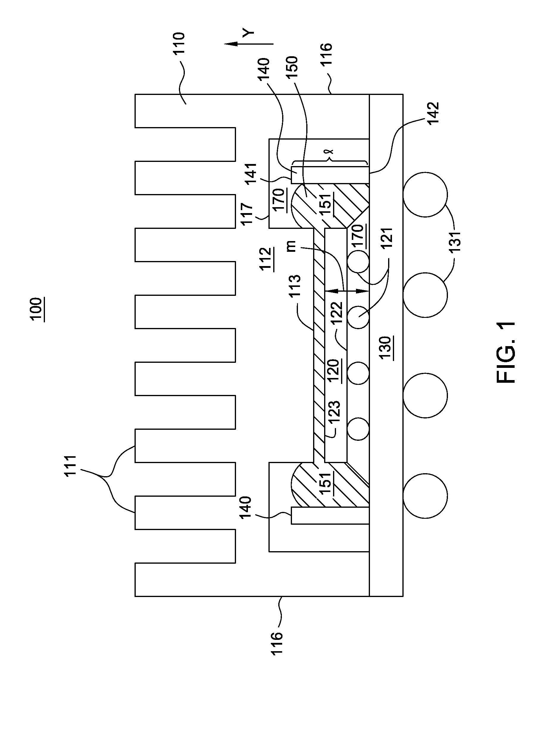
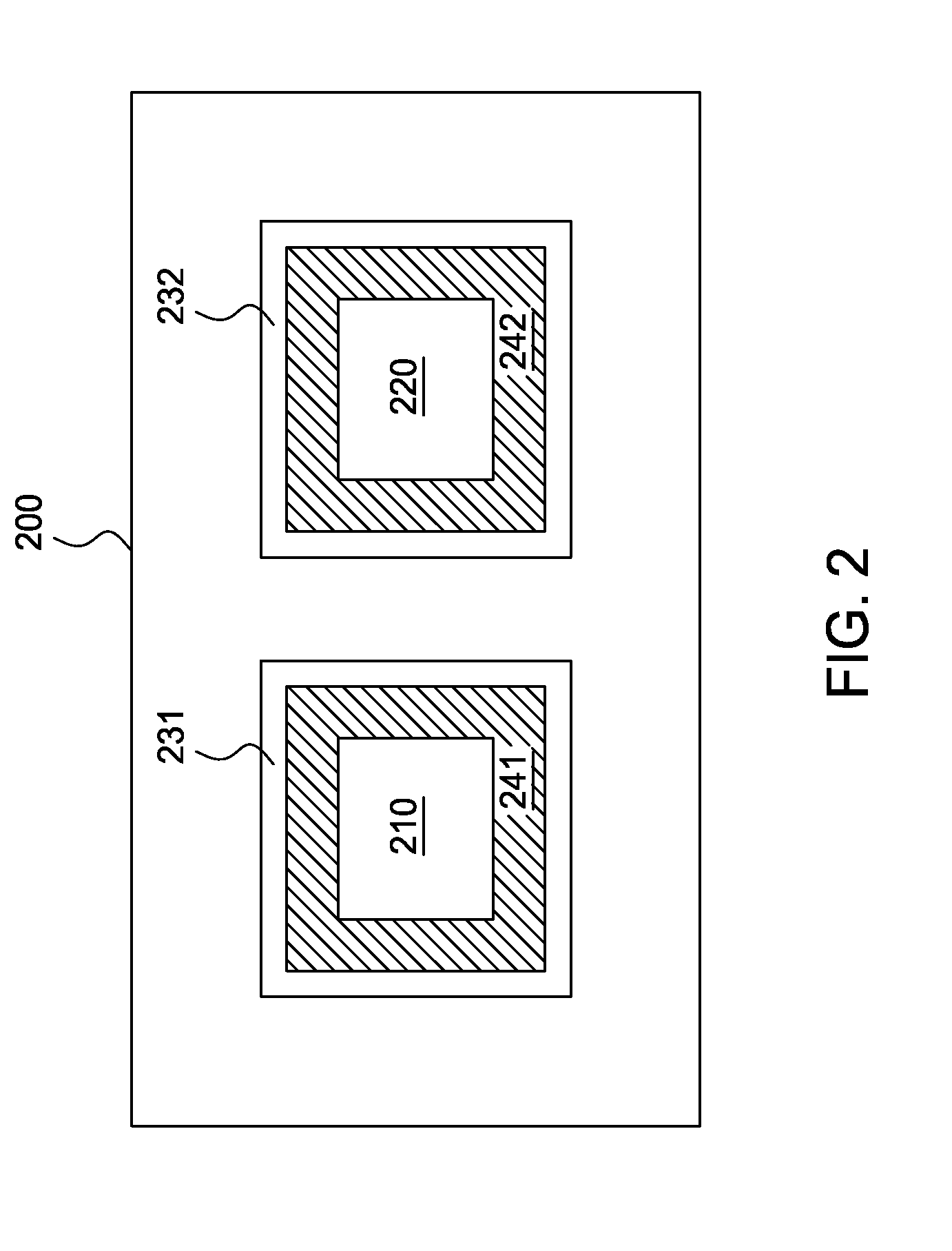
[0017]Embodiments of the invention are generally related to packaging of integrated circuit devices, and more specifically to the placement of thermal paste for cooling an integrated circuit device during operation. A barrier element may be placed along at least one side of an integrated circuit chip. The barrier element may contain thermal paste pumped out during expansion and contraction of the package components to areas near the chip. The barrier element may also form a reservoir to replenish thermal paste that is lost during thermal pumping of the paste.

[0018]In the following, reference is made to embodiments of the invention. However, it should be understood that the invention is not limited to specific described embodiments. Instead, any combination of the following features and elements, whether related to different embodiments or not, is contemplated to implement and practice the invention. Furthermore, although embodiments of the invention may achieve advantages over other...


PUM


Abstract

Embodiments of the invention are generally related to packaging of integrated circuit devices, and more specifically to the placement of thermal paste for cooling an integrated circuit device during operation. A barrier element may be placed along at least one side of an integrated circuit chip. The barrier element may contain thermal paste pumped out during expansion and contraction of the package components to areas near the chip. The barrier element may also form a reservoir to replenish thermal paste that is lost during thermal pumping of the paste.

Description

BACKGROUND OF THE INVENTION[0001]1. Field of the Invention[0002]The present invention is generally related to packaging of integrated circuit devices, and more specifically providing a thermal paste for cooling an integrated circuit device during operation.[0003]2. Description of the Related Art[0004]Since the invention of the transistor, dissipation of heat during operation has been an important consideration in semiconductor device package design. Heat can damage the delicate and tiny structures which allow transistors to function as intended in a semiconductor device. Power drawn by transistors and other electronic devices must be dissipated to avoid build up of heat and the development of high temperatures which can degrade the devices by such mechanisms as dopant diffusion, metal migration including solder softening and reflow, or the like.[0005]As semiconductor devices become smaller and smaller, it has become more difficult to provide efficient heat dissipation mechanisms. Cu...

Claims


Application Information

Patent Timeline
IPC IPC(8): H01L23/29H01L21/50H01L23/52
CPCH01L21/563H01L21/565H01L2224/32225H01L2224/16225H01L2924/19041H01L2924/16152H01L2924/15311H01L2224/73204H01L2224/73203H01L23/42H01L23/293H01L23/296H01L23/3128H01L23/3135H01L23/3675H01L2924/00H01L2224/73253
Inventor EDWARDS, DAVID L.LANDREVILLE, JEAN-LUCLANGE, KATHRYN R.SAVARD, CARLSIKKA, KAMLA K.TOY, HILTON T.
Owner GLOBALFOUNDRIES INC
Learn More