Method for fabricating robust light-emitting diodes

Inactive Publication Date: 2011-03-03
LATTICE POWER (JIANGXI) CORP
View PDF3 Cites 95 Cited by
  • Summary
  • Abstract
  • Description
  • Claims
  • Application Information

AI Technical Summary

Benefits of technology

[0009]One embodiment of the present invention provides a method for fabricating light-emitting diodes (LEDs). The method includes fabricating an InGaAlN-based multilayer LED structure on a conductive substrate. The method further includes etching grooves of a predetermined pattern through the active region of the multilayer LED structure. The grooves separate a light-emitting region from non-light-emitting regions. In addition, the method includes depositing electrode material on the light-emitting and non

Problems solved by technology

However, the bond formed between the InGaAlN-based multilayer structure and the conductive substrate may not always be sufficiently strong to withstand the subsequent processing and testing.
Specifically, the bond created by pressure-welding two unevenly surfaced bonding materials reduces the integrity of the contact surface and weakens the bond st

Method used


Image

  • Method for fabricating robust light-emitting diodes
  • Method for fabricating robust light-emitting diodes
  • Method for fabricating robust light-emitting diodes

Examples


Embodiment Construction

[0033]The following description is presented to enable any person skilled in the art to make and use the invention, and is provided in the context of a particular application and its requirements. Various modifications to the disclosed embodiments will be readily apparent to those skilled in the art, and the general principles defined herein may be applied to other embodiments and applications without departing from the scope of the present invention. Thus, the present invention is not limited to the embodiments shown, but is to be accorded the widest scope consistent with the claims.

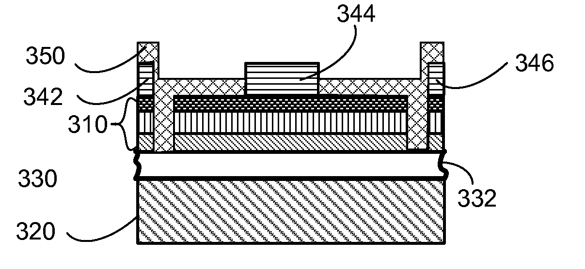
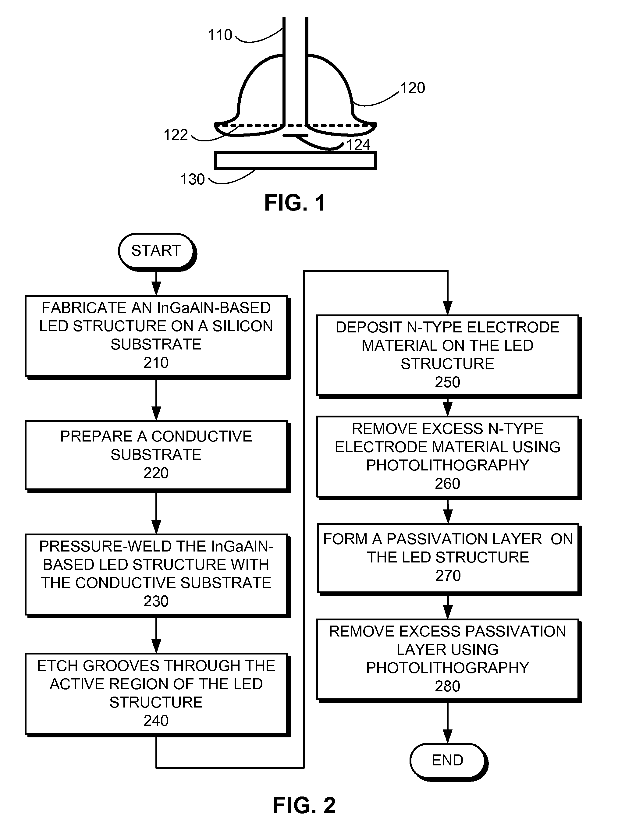
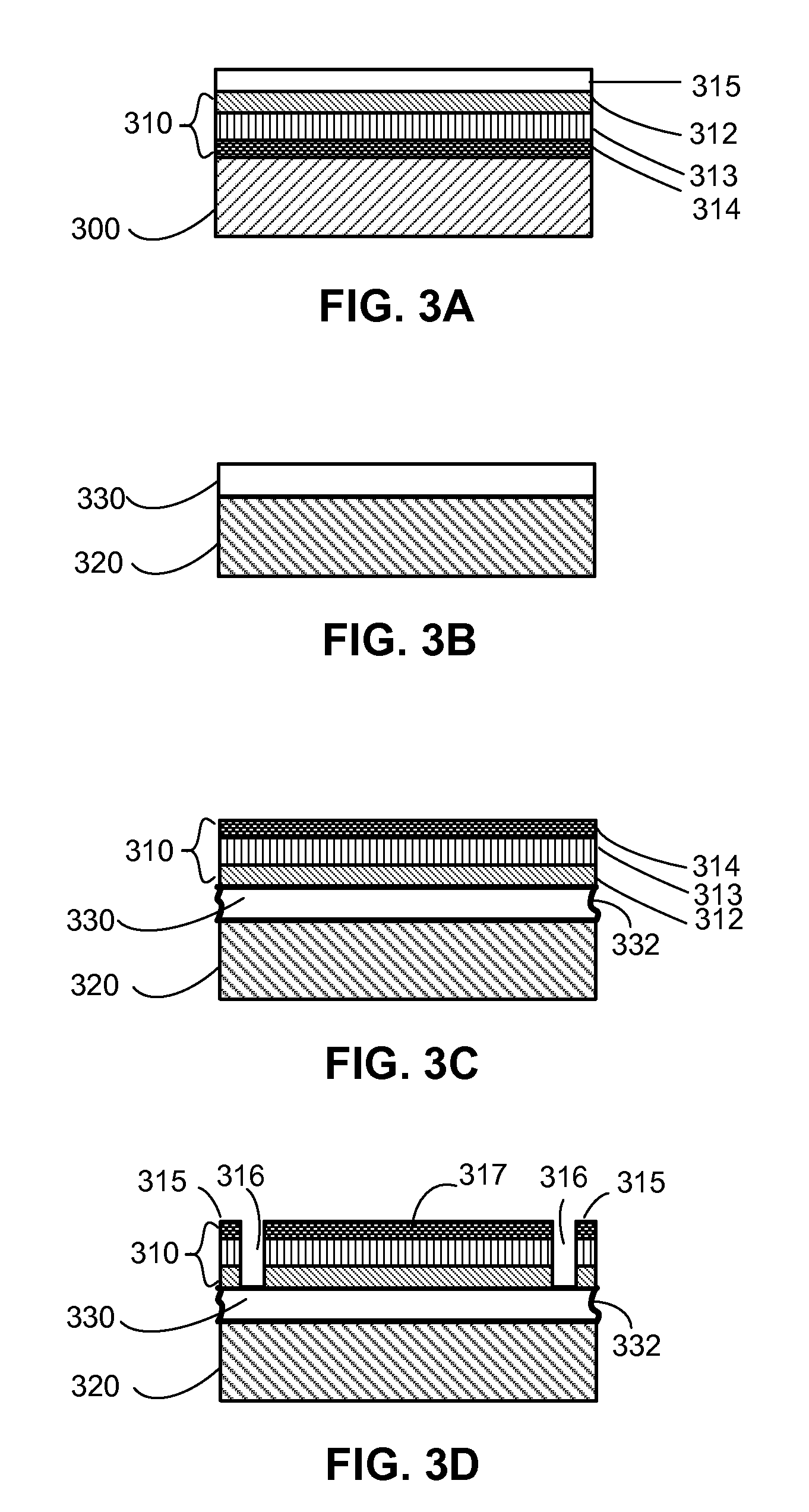
[0034]Embodiments of the present invention provide a method for manufacturing high-quality light-emitting diodes (LEDs) while minimizing the risk of damaging LEDs in the testing process. Typically, after the LED structures are fabricated on a substrate, the wafer is diced to separate individual LEDs, which undergo further processes including testing and packaging. Each LED is moved around in the product...


PUM


Abstract

One embodiment of the present invention provides a method for fabricating light-emitting diodes (LEDs). The method includes fabricating an InGaAlN-based multilayer LED structure on a conductive substrate. The method further includes etching grooves of a predetermined pattern through the active region of the multilayer LED structure. The grooves separate a light-emitting region from non-light-emitting regions. In addition, the method includes depositing electrode material on the light-emitting and non-light-emitting regions, thereby creating an electrode. Furthermore, the method includes depositing a passivation layer covering the light-emitting and non-light-emitting regions. Moreover, the method includes removing the passivation layer on the electrode to allow the non-light-emitting regions which are covered with the electrode material and the passivation layer to be higher than the light-emitting region and the electrode, thereby protecting the light-emitting region from contact with test equipment.

Description

RELATED APPLICATION[0001]This application is a national-stage application of and hereby claims priority under 35 U.S.C. §120, §365(c), and §371 to PCT Application No PCT / CN2008 / 000596, filed 26 Mar. 2008.BACKGROUND[0002]1. Field of the Invention[0003]The present invention relates to the manufacturing of semiconductor light-emitting devices using InGaAlN-based (InxGa1-xAlyN1-y, 0<=x<=1, 0<=y<=1) semiconductor material. More specifically, the present invention relates to a technique for minimizing the risk of damaging epitaxially fabricated InGaAlN-based light-emitting diodes during back side processing, testing, and packaging.[0004]2. Related Art[0005]Group III-V nitride compounds (e.g., GaN, InN, and AlN) and alloy compounds (e.g., AlGaN, InGaN, and AlGaInN) have been widely used in the manufacturing of light-emitting diodes (LEDs) and laser diodes that generate efficient luminescence. Techniques for epitaxially growing LEDs with group III-V nitride material include meta...

Claims


Application Information

Patent Timeline
IPC IPC(8): H01L33/32H01L21/18H01L33/20H01L33/44H01L33/62
CPCH01L33/20H01L33/44H01L33/62H01L2924/0002H01L2924/00
Inventor WANG, LIJIANG, FENGYI
Owner LATTICE POWER (JIANGXI) CORP
Why Eureka
Try Eureka