Substrate cartridge, substrate processing apparatus, substrate processing system, control apparatus, and method of manufacturing display element
- Summary
- Abstract
- Description
- Claims
- Application Information
AI Technical Summary
Benefits of technology
Problems solved by technology
Method used
Image

Examples
Embodiment Construction
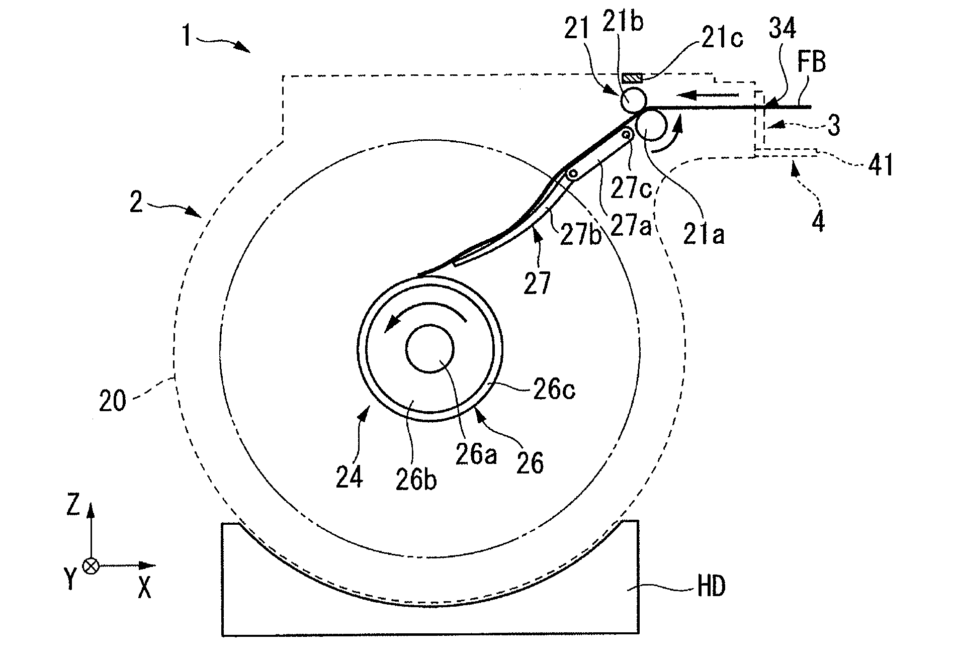
[0063]Hereinafter, an embodiment of the present invention will be described with reference to the accompanying drawings.
[0064](Organic EL Element)
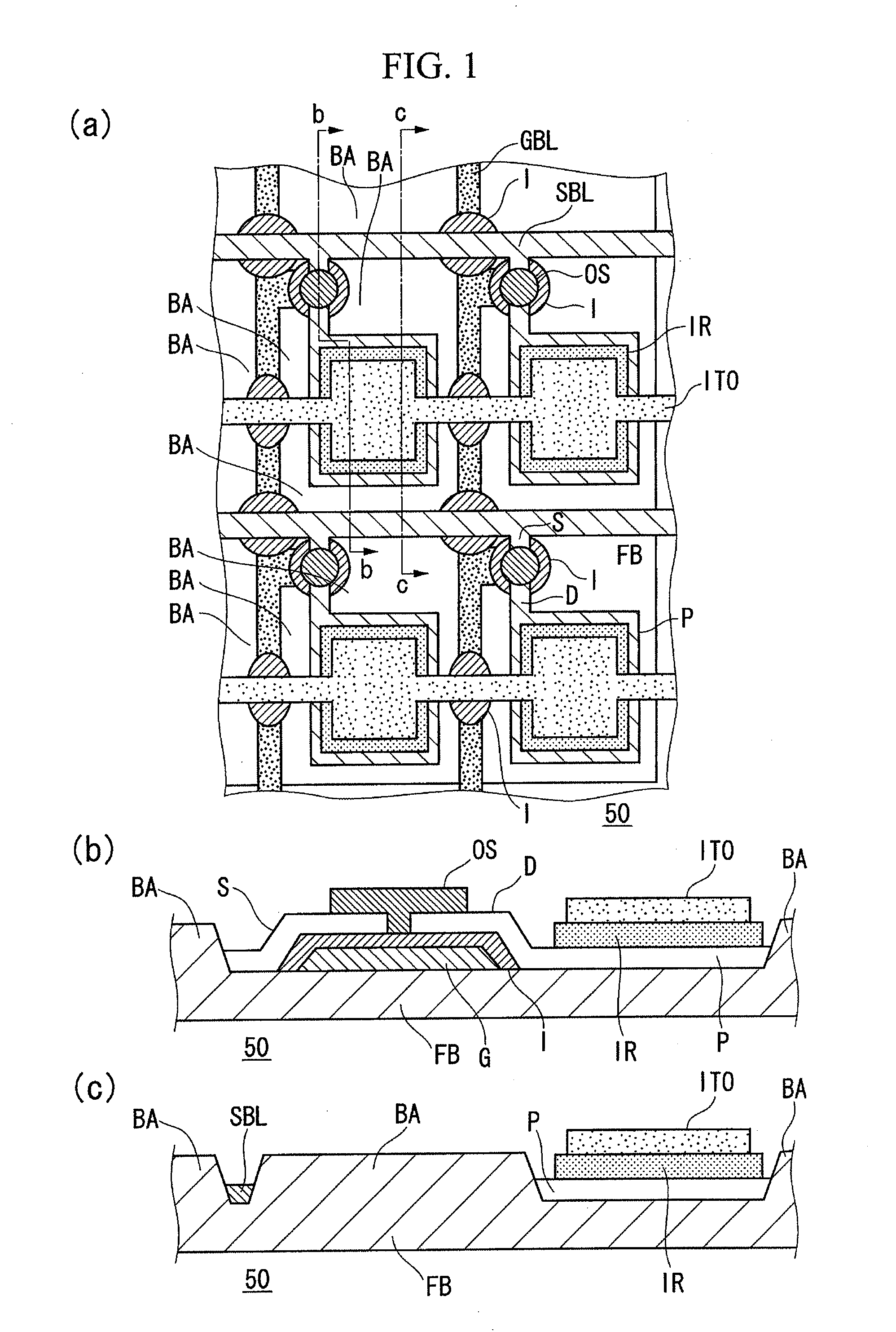
[0065]FIG. 1(a) is a plan view illustrating a configuration of the organic EL element. FIG. 1(b) is a cross-sectional view taken along the line b-b of FIG. 1(a). FIG. 1(c) is a cross-sectional view taken along the line c-c of FIG. 1(a).
[0066]As shown in FIGS. 1(a) to 1(c), the organic EL element 50 is a bottom contact type in which the gate electrode G and the gate insulation layer I are formed on the sheet substrate FB. Further, the source electrode S, the drain electrode D and the pixel electrode P are formed thereon, and then, the organic semiconductor layer OS is formed thereon.
[0067]As shown in FIG. 1(b), the gate insulation layer I is formed on the gate electrode G. On the gate insulation layer I, the source electrode S of the source bus line SBL is formed, and at the same time, the drain electrode D connected to the pixel electrode ...
PUM
| Property | Measurement | Unit |
|---|---|---|
| Radius | aaaaa | aaaaa |
| Electric properties | aaaaa | aaaaa |
| Transport properties | aaaaa | aaaaa |
Abstract
Description
Claims
Application Information
 - R&D Engineer
- R&D Manager
- IP Professional
- Industry Leading Data Capabilities
- Powerful AI technology
- Patent DNA Extraction
Browse by: Latest US Patents, China's latest patents, Technical Efficacy Thesaurus, Application Domain, Technology Topic.
© 2024 PatSnap. All rights reserved.Legal|Privacy policy|Modern Slavery Act Transparency Statement|Sitemap