

Method for imaging workpiece surfaces at high robot transfer speeds with correction of motion-induced distortion
a technology of workpiece surfaces and robots, which is applied in the field of high robot transfer speed imaging workpiece surfaces with correction of motion-induced distortion, can solve the problems of affecting the accuracy of in-situ measurement of the width or concentricity of the film edge exclusion annular region, and affecting the true circular shape of the wafer
- Summary
- Abstract
- Description
- Claims
- Application Information
AI Technical Summary
Problems solved by technology
Method used
Image

Examples
Embodiment Construction
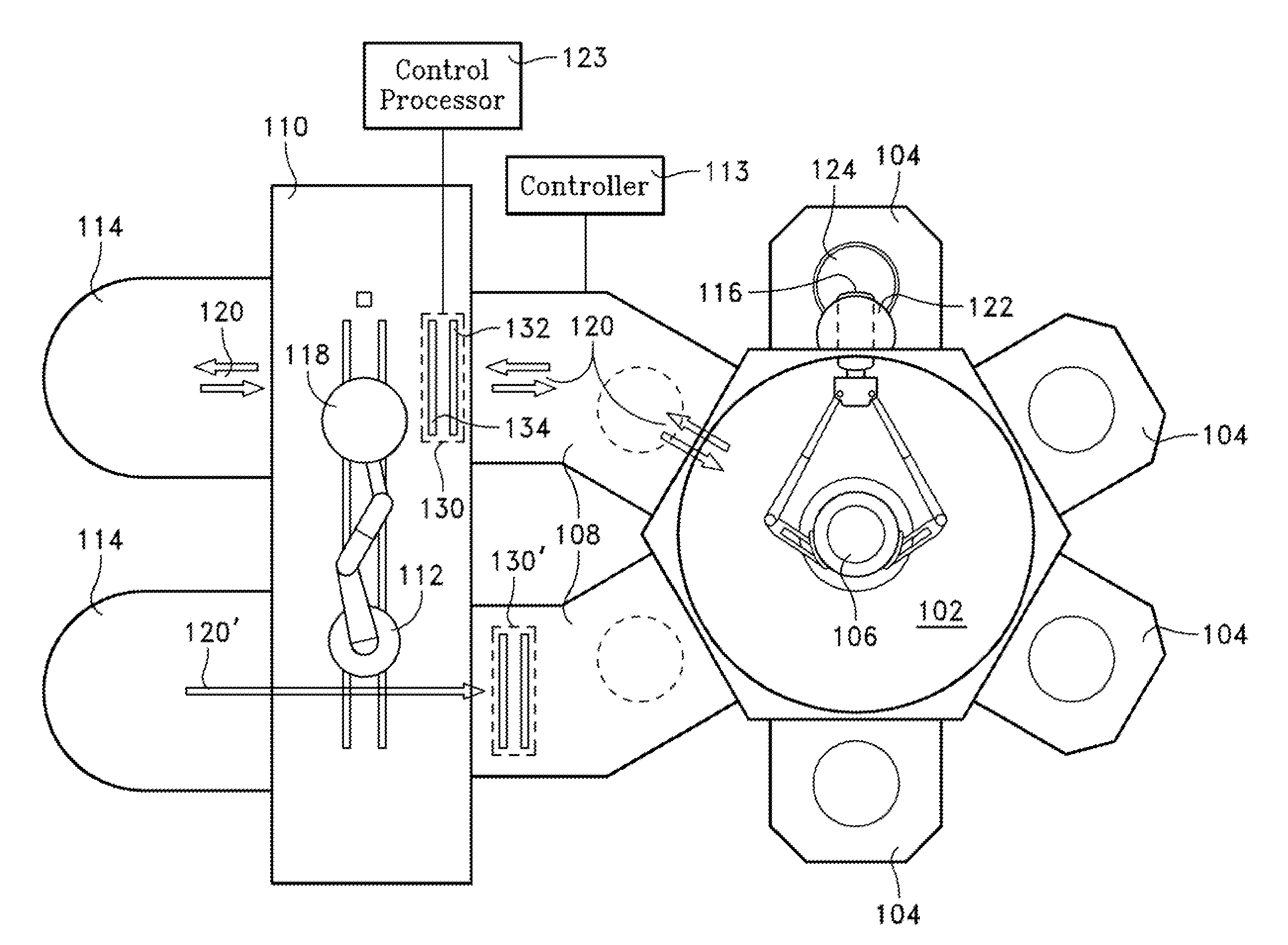
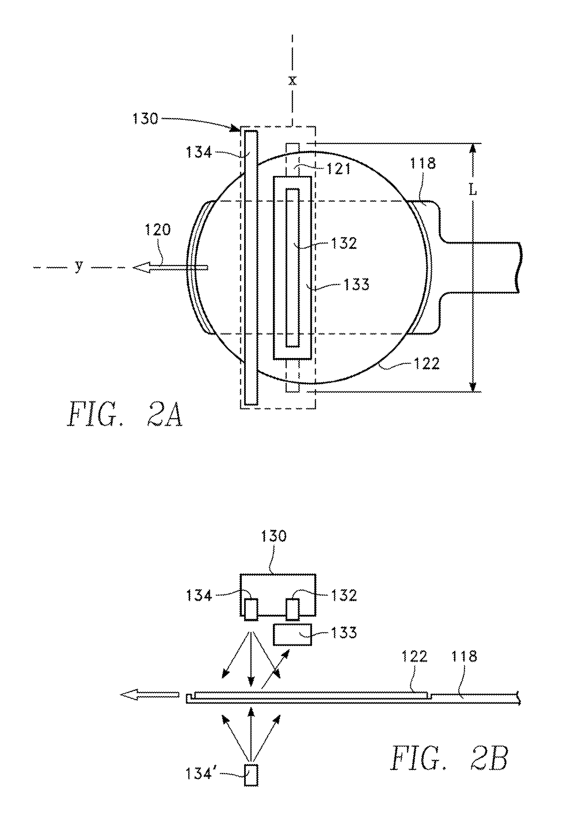
FIG. 1 depicts a wafer processing tool that includes a vacuum transfer chamber 102 coupled to four wafer processing chambers 104, all held at sub-atmospheric pressure. A vacuum robot 106 transfers individual wafers between any one of the processing chambers 104 and any one of two load lock chambers 108. A factory interface 110 is at atmospheric pressure, and includes an atmospheric robot 112 for transferring a wafer between one or more cassettes 114 and the load lock chamber 108. The load lock chamber 108 provides a transition between the atmospheric pressure of the factory interface 110 and the vacuum of the vacuum transfer chamber 102. The vacuum robot 106 holds each wafer on a vacuum robot blade 116, while the atmospheric robot 112 holds each wafer on an atmospheric robot blade 118. The robots 106, 112 move each wafer along a wafer transit path 120 through the factory interface at a high speed of over 1 meter per second, e.g., about 1.7 meters per second. The robots 106, 112 are ...
PUM
 Abstract
Description
Claims
Application Information