Display device and method for driving the same

a technology which is applied in the field of display device and drive transistor, can solve the problems of deteriorating image quality characteristics, unfavorable, and reduced weight of flat panel display device, and achieve the effect of accurately measuring the variation in characteristics of driving transistor

Active Publication Date: 2011-10-20
SAMSUNG DISPLAY CO LTD
View PDF4 Cites 68 Cited by
  • Summary
  • Abstract
  • Description
  • Claims
  • Application Information

AI Technical Summary

Benefits of technology

[0012]The present invention has been made in an effort to provide a display device that can accurately measure variations in characteristics of driving transistors of a pixel circuit of different pixels and compensate for these variations more precisely.
[0014]The compensator may include a measurement unit to measure the first and second pixel current of the pixels, a target unit to eliminate noise generated by the measurement unit, a comparator to compare output values of the measurement unit and the target unit and a successive approximation register (SAR) logic to process an output value of the comparator. The measurement unit may include the measurement resistor and a differential amplifier to output a difference between a predetermined test data voltage and the voltage converted from the first and second pixel currents. The differential amplifier may include a non-inverting input terminal to receive the first and second data voltages, an inverting input terminal to receive the voltage converted from the first and second pixel currents and an output terminal to output a difference between one of the first and second data voltage and the voltage converted from the corresponding one of the first and second pixel current.

Problems solved by technology

Recently, various flat panel display devices having reduced weight and volume, which are unfavorable aspects of a cathode ray tube, have been developed.
As a result, the moiré phenomenon occurs, and thereby image quality characteristics are deteriorated.

Method used


Image

  • Display device and method for driving the same
  • Display device and method for driving the same
  • Display device and method for driving the same

Examples


Embodiment Construction

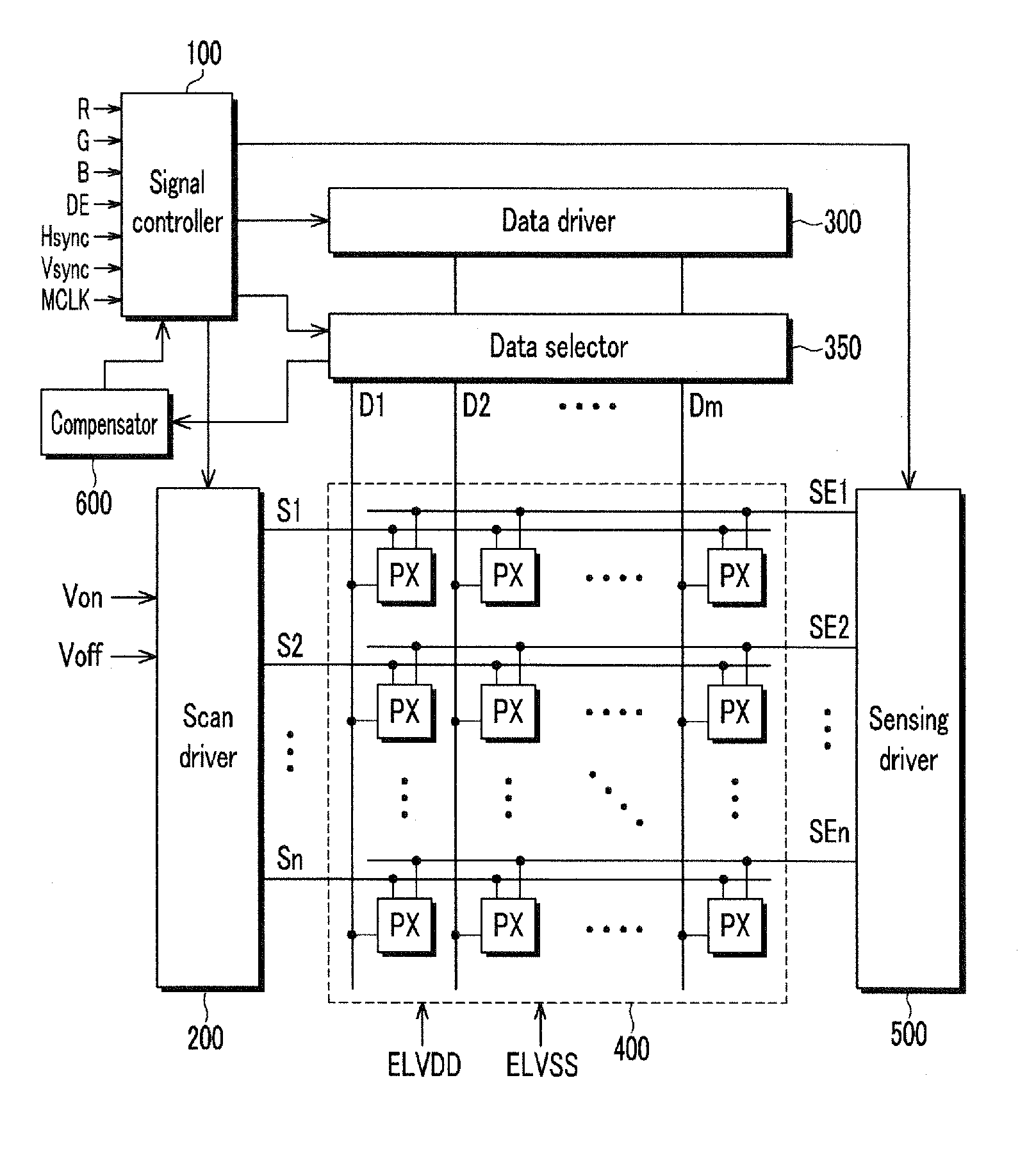
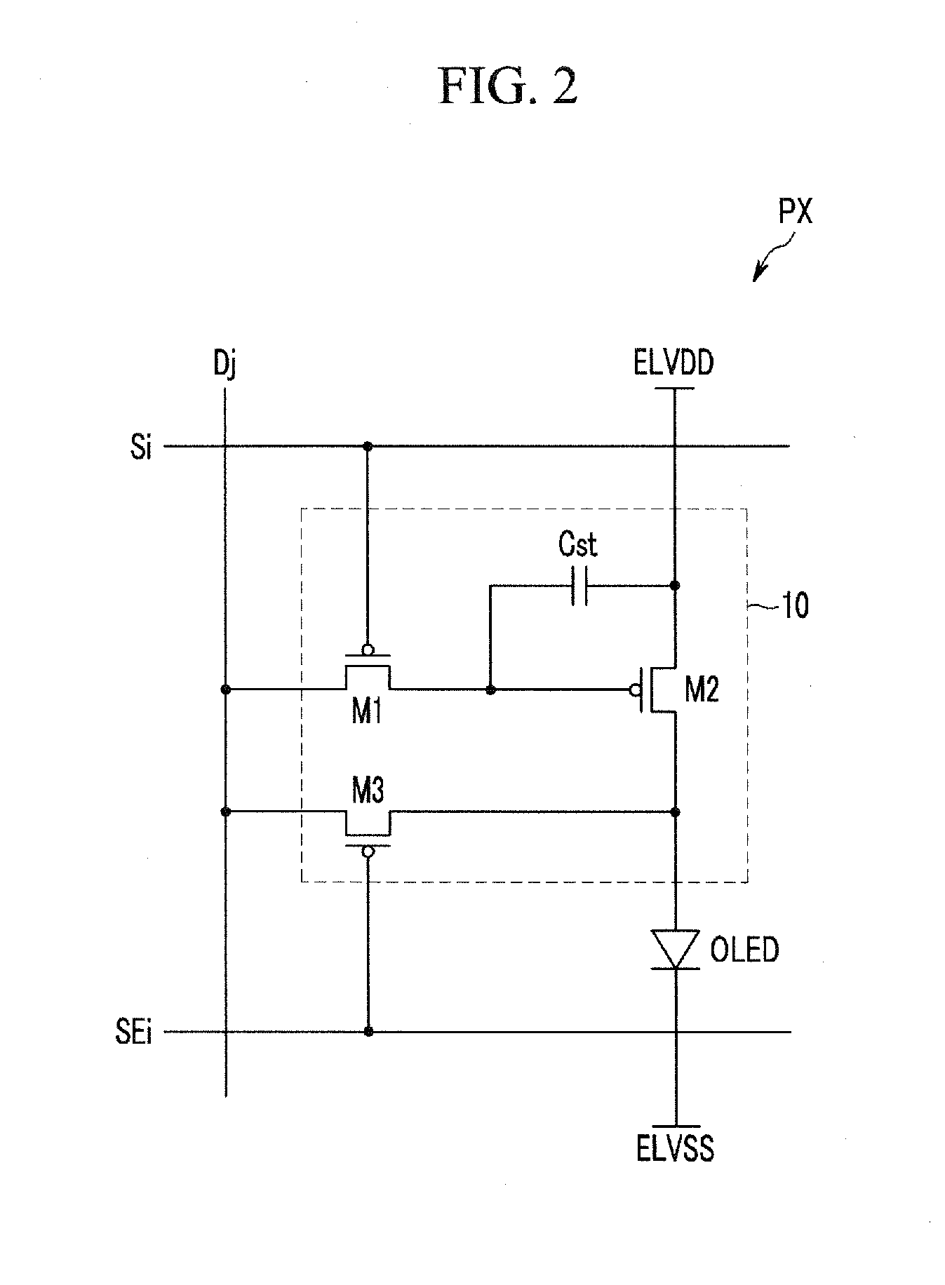
[0027]Exemplary embodiments of the invention will now be described in detail such that those skilled in the art can easily implement it with reference to the accompanying drawings. As those skilled in the art would realize, the described embodiments may be modified in various different ways, all without departing from the spirit or scope of the present invention.

[0028]Constituent elements having the same structures throughout the embodiments are denoted by the same reference numerals and are described in a first exemplary embodiment. In the other exemplary embodiments, only other constituent elements are described. To clearly describe the exemplary embodiments of the present invention, parts not related to the description are omitted, and like reference numerals designate like constituent elements throughout the specification.

[0029]Throughout this specification and the claims that follow, when it is described that an element is “coupled” to another element, the element may be “direc...


PUM


Abstract

A display device includes a plurality of pixels, each of said plurality of pixels includes a driving transistor and a light emitting diode, a compensator to receive first and second pixel currents generated by the plurality of pixels according to first and second data voltages respectively applied to the plurality of pixels, the compensator to calculate an image data compensation amount to compensate for variations in characteristics of the driving transistor of each of said plurality of pixels and a data selector to transmit the first and second data voltages to the plurality of pixels and to transmit the first and second pixel currents to the compensator, the compensator to measure the first and second pixel currents generated as a result of the first and second data voltages corresponding to different gray scale levels and to calculate an actual threshold voltage and mobility of the driving transistor of each of the pixels, the compensator including a measurement resistor, the compensator to control a resistance value of the measurement resistor, the measurement resistor to convert the first pixel current corresponding to the first data voltage into a first measured voltage and the second pixel current corresponding to the second data voltage into a second measured voltage.

Description

CLAIM OF PRIORITY[0001]This application makes reference to, incorporates the same herein, and claims all benefits accruing under 35 U.S.C. §119 from an application earlier filed in the Korean Intellectual Property Office on Apr. 14, 2010 and there duly assigned Serial No. 10-2010-0034329.BACKGROUND OF THE INVENTION[0002]1. Field of the Invention[0003]The present invention relates to a display device that compensates for variations in characteristics of driving transistors of pixels and a method of driving the same.[0004]2. Description of the Related Art[0005]Recently, various flat panel display devices having reduced weight and volume, which are unfavorable aspects of a cathode ray tube, have been developed. Examples of flat panel display devices include liquid crystal displays, field emission displays, plasma display panels, organic light emitting displays, and others.[0006]Among these flat panel display devices, the organic light emitting display displays images using an organic l...

Claims


Application Information

Patent Timeline
Patent Type & Authority Applications(United States)
IPC IPC(8): G09G3/32G09G5/10
CPCG09G3/3233G09G2320/043G09G2320/0295G09G2300/043
Inventor YOO, MYOUNG-HWANOH, CHOON-YULKOMIYA, NAOAKICHUNG, HO-RYUNJEONG, JOO-HYEONLEE, WANG-JOCHOI, IN-HOHYUN, CHANG-HOKIM, WOUNG
Owner SAMSUNG DISPLAY CO LTD
Why Eureka
Try Eureka