Substrate for an optical device, an optical device package comprising the same and a production method for the same
Inactive Publication Date: 2011-11-17
POINT ENG
View PDF9 Cites 25 Cited by
Summary
Abstract
Description
Claims
Application Information
AI Technical Summary
This helps you quickly interpret patents by identifying the three key elements:
Problems solved by technology
Method used
Benefits of technology
Benefits of technology
[0015]The present invention is advantageous in that the heat emitted from an optical device can be efficiently discharged to the outside using a metal substrate.
[0016]Further, the present invention is advantageous in that the thickness of an anodized lay
Problems solved by technology
LEDs are advantageous in that they have high luminance and high energy efficiency, but are problematic in that they generate a large amount of heat.
However, when a heat sink is used, there is a problem in that the size of an LED package increases and in that additional processes must be performed.
Furt
Method used
Image
Click on the blue label to locate the original text in one second.
Reading with bidirectional positioning of images and text.
Examples
Example
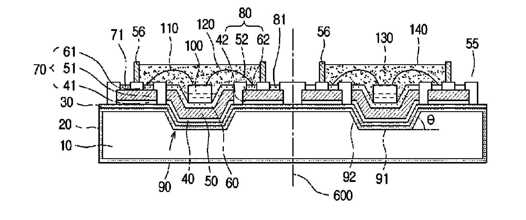
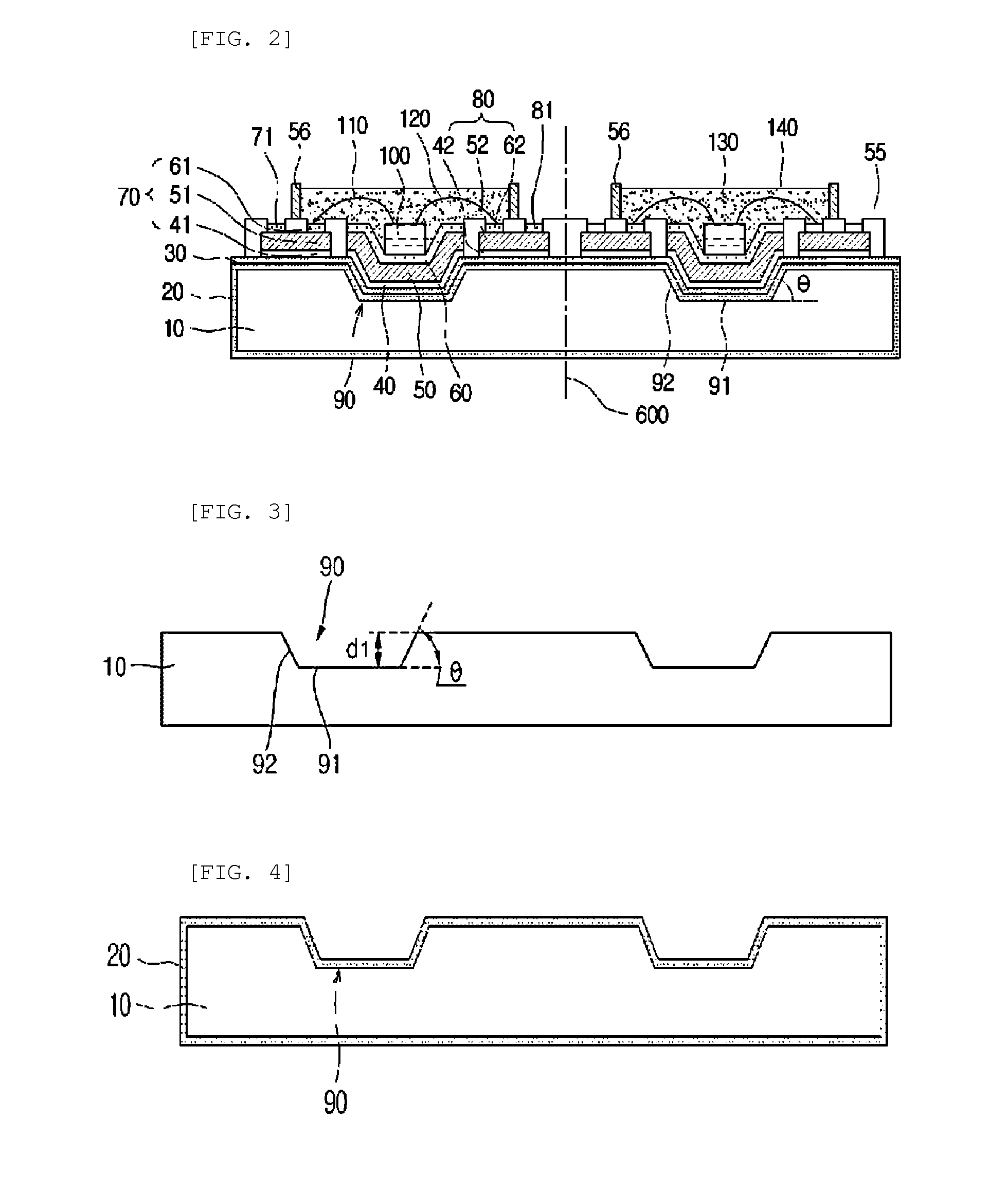
[0098]Referring to FIG. 14, the light emitting diode package according to the second embodiment of the present invention includes a substrate 400 for a light emitting diode, a light emitting diode 100, a first wire 110, and a second wire 120. Here, the substrate 400 for a light emitting diode may include a metal substrate 10, a reflecting recess 90, a first anodized layer 20, a second anodized layer 30, a photo solder resist pattern 55, first to fourth electrodes 70, 80, 71 and 81, and side walls 56.
[0099]Concretely, the metal substrate 10 may be made of aluminum, titanium, magnesium, zinc, niobium or an alloy thereof.
[0100]At least one reflecting recess 90 may be formed on one side of the metal substrate 10. The reflecting recess 90 is formed in such a way that the metal substrate 10 is depressed. The reflecting recess 90 may be formed in the shape of a circle. However, the reflecting recess 90 may be formed in the shape of a polygon such as a triangle, a quadrangle or the like wit...
Example
[0128]Concretely, the light emitting diode package according to the third embodiment of the present invention includes a substrate 400 for a light emitting diode, a light emitting diode 100. Here, the substrate 400 for a light emitting diode may include a metal substrate 10, and a first anodized layer 20 formed on the metal substrate 10. Further, the substrate 400 for a light emitting diode may further include a second anodized layer 30 formed on the first anodized layer 20.
[0129]The substrate 400 for a light emitting diode may include first to fourth electrodes 70, 80, 71 and 81. Since these first to fourth electrodes 70, 80, 71 and 81 are the same as those shown in FIG. 2, description thereof will be omitted.
[0130]A light emitting diode 100 is mounted on a third metal layer 60, and a first wire 110 is connected with a first electrode by soldering or the like.
[0131]A protection layer 130 is made of a mixture of phosphor and epoxy to cover the light emitting diode 100. A protection ...
PUM
Abstract
The present invention relates to a substrate for an optical device, to an optical device package comprising the same and to a production method for the same. According to the present invention, the substrate for an optical device, the optical device package comprising the same and the production method for the same may comprise: a metal substrate; a first anodized layer which is formed on the top surface of the metal substrate and insulates the metal substrate; and a first and a second electrode formed insulated from each other on the top of the first anodized layer.
Description
TECHNICAL FIELD[0001]The present invention relates to a substrate for an optical device, an optical device package comprising the substrate, and a method of manufacturing the optical device package.BACKGROUND ART[0002]An optical device serves to convert electric energy into light or light energy into electric energy, and has various sizes and shapes depending on the intended use.[0003]Recently, among optical devices, a light emitting diode (hereinafter, referred to as ‘LED’) has been generally used in the field of illumination, displays or the like. An LED is mounted on a printed circuit board, and is used in the form of a single device or an array. LEDs are advantageous in that they have high luminance and high energy efficiency, but are problematic in that they generate a large amount of heat.[0004]In order to solve the above problem of heat generation, conventionally, a heat sink has been provided at the lower portion of an LED package, or metal pads for thermal conduction have b...
Claims
Application Information
Patent Timeline
Application Date:The date an application was filed.
Publication Date:The date a patent or application was officially published.
First Publication Date:The earliest publication date of a patent with the same application number.
Issue Date:Publication date of the patent grant document.
PCT Entry Date:The Entry date of PCT National Phase.
Estimated Expiry Date:The statutory expiry date of a patent right according to the Patent Law, and it is the longest term of protection that the patent right can achieve without the termination of the patent right due to other reasons(Term extension factor has been taken into account ).
Invalid Date:Actual expiry date is based on effective date or publication date of legal transaction data of invalid patent.

