Test apparatus, test method, and device interface

a test apparatus and test method technology, applied in the direction of optical elements, instruments, optical radiation measurement, etc., can solve the problems of increasing manufacturing cost, increasing testing cost, and reducing throughput of testing

Active Publication Date: 2011-11-17
ADVANTEST CORP
View PDF11 Cites 27 Cited by
  • Summary
  • Abstract
  • Description
  • Claims
  • Application Information

AI Technical Summary

Problems solved by technology

The test apparatus requires accurate adjustment of the optical axis of the optical input and output, and this decreases the throughput of the testing while increasing the testing cost.
In this case, if the device under test does not perform as desired, the package must be rejected along with the device under test, thereby increasing the manufacturing cost.

Method used


Image

  • Test apparatus, test method, and device interface
  • Test apparatus, test method, and device interface
  • Test apparatus, test method, and device interface

Examples


Embodiment Construction

[0012]Hereinafter, some embodiments of the present invention will be described. The embodiments do not limit the invention according to the claims, and all the combinations of the features described in the embodiments are not necessarily essential to means provided by aspects of the invention.

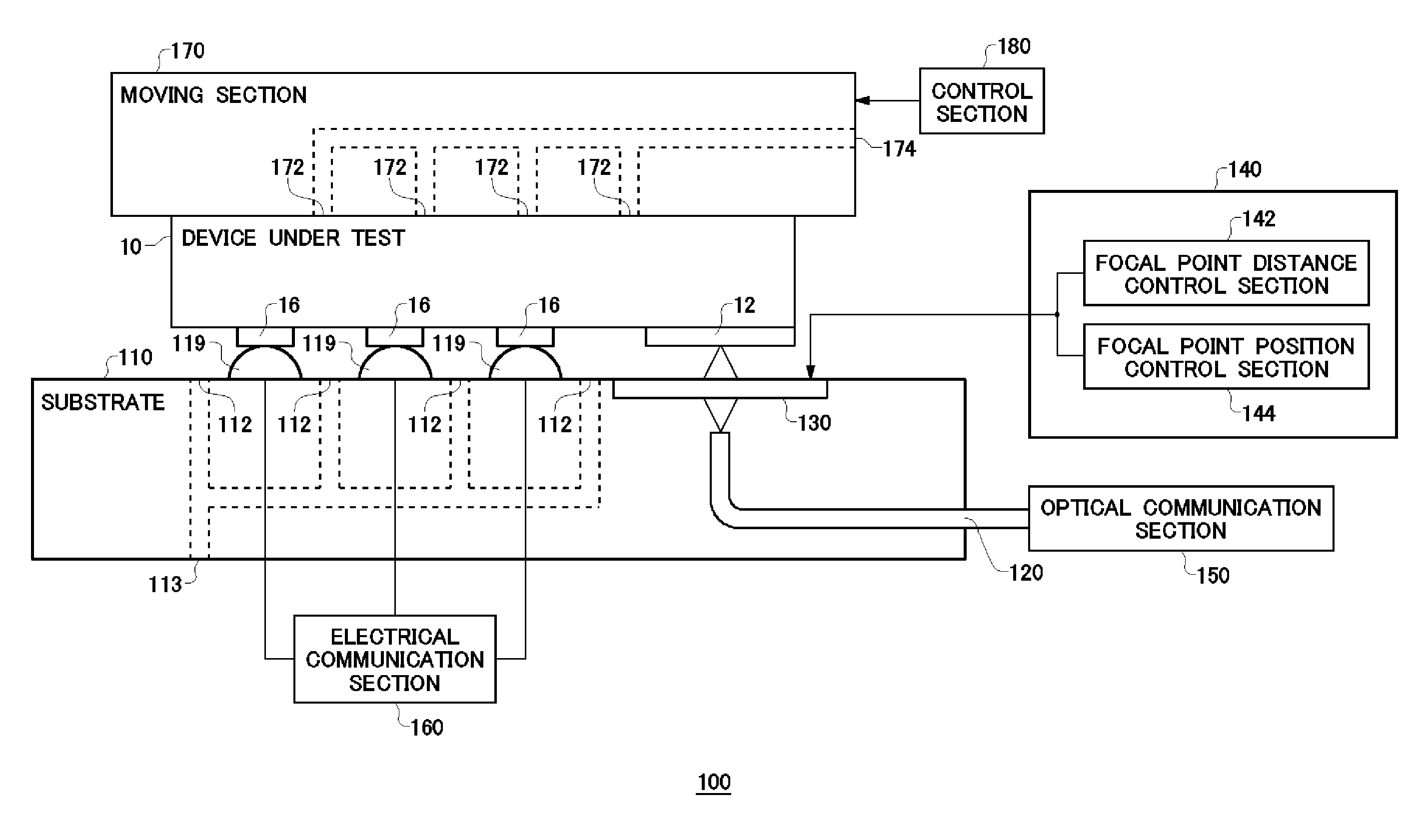
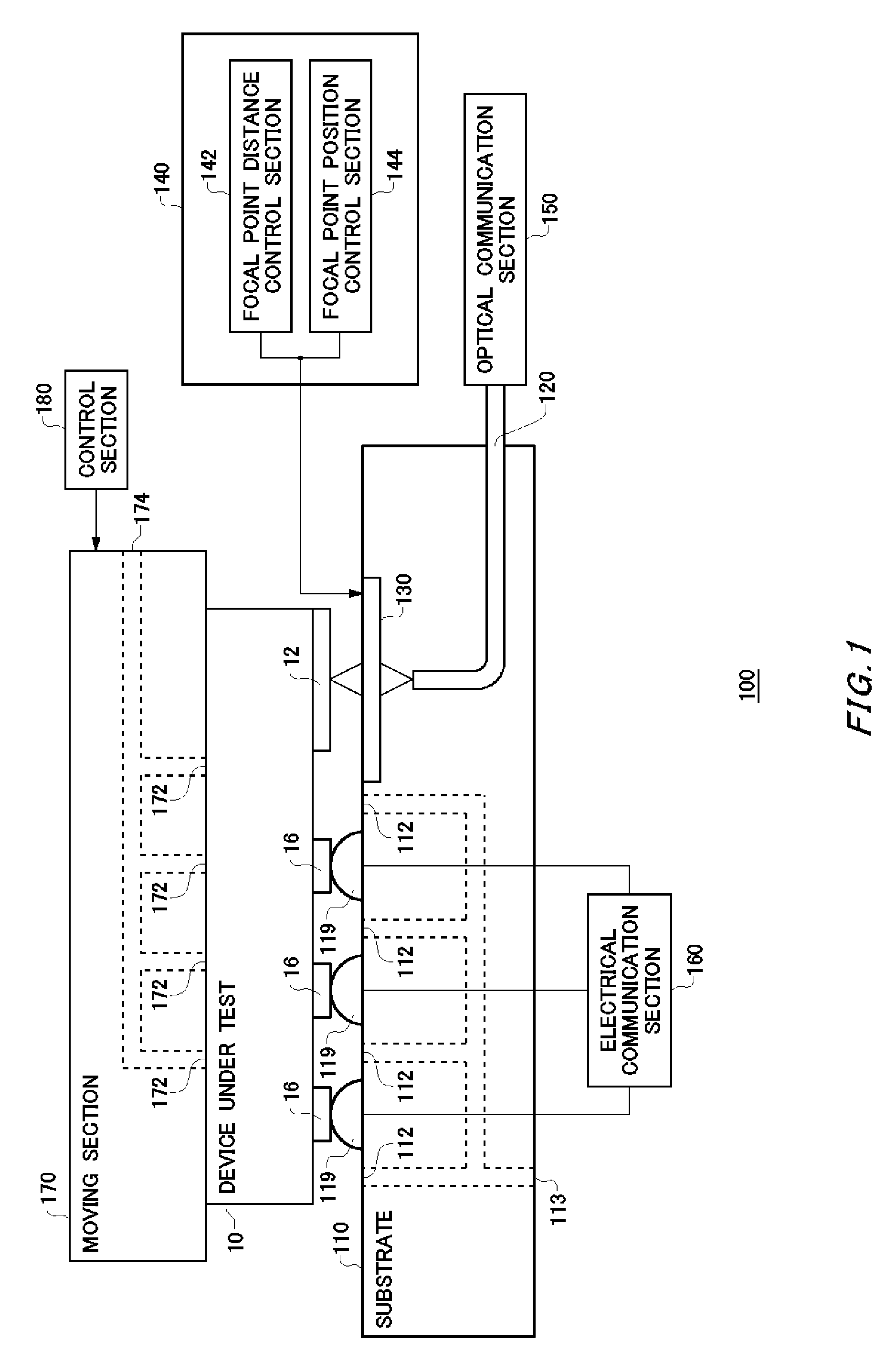
[0013]FIG. 1 shows an exemplary configuration of an interface between a device under test 10 and a test apparatus 100, according to an embodiment of the present invention. The test apparatus 100 exchanges optical signals and electrical signals with the device under test 10 having an optical interface to test the device under test 10, which may be an analog circuit, a digital circuit, a memory, or a system on chip (SOC), for example. The device under test 10 includes an optical coupler 12. The device under test 10 may include terminals 16.

[0014]The optical coupler 12 transmits optical signals in a direction perpendicular to the device surface. The optical coupler 12 may be optically coupled to a...


PUM


Abstract

Provided is a test apparatus that tests a device under test including an optical coupler transmitting optical signals in a direction perpendicular to a device surface. The test apparatus comprises a substrate on which the device under test is to be loaded; an optical transmission path that transmits the optical signals: and a lens section that is provided facing the optical coupler on the substrate and that focuses the optical signals from an end of one of the optical coupler and the optical transmission path to an end of the other.

Description

BACKGROUND[0001]1. Technical Field[0002]The present invention relates to a test apparatus, a test method, and a device interface.[0003]2. Related Art[0004]Conventionally, a test apparatus is used to test a device under test such as a CPU or a memory. The device under test can be provided with an optical interface, as shown in Patent Document 1 and Non-Patent Documents 1 and 2, for example.Patent Document 1: International Publication WO 2007 / 013128 Non-Patent Document 1: Ian A. Young, et al., “Optical I / O Technology for Tera-Scale Computing”, IEEE Journal of Solid-State Circuits, January 2010, Vol. 45, No. 1, pp. 235-248 [0005]Non-Patent Document 2: Hiren D. Thacker, James D. Meindl, “Prospects for Wafer-Level Testing of Gigascale Chips with Electrical and Optical I / O Interconnects”, IEEE International Test Conference, 2006, 25-1Non-Patent Document 3: Shin Masuda, et al., “Liquid-crystal microlens with a beam-steering function”, APPLIED OPTICS, July 1997, Vol. 36, No. 20, pp. 4772-...

Claims


Application Information

Patent Timeline
Patent Type & Authority Applications(United States)
IPC IPC(8): G01J1/00G01R19/00
CPCG01J1/28G01R15/22G02B6/4206G01R31/311G01R31/2886
Inventor MASUDA, SHIN
Owner ADVANTEST CORP
Why Eureka
Try Eureka