Plasma Processing Chamber with Dual Axial Gas Injection and Exhaust

a technology of gas injection and processing chamber, which is applied in the direction of electric discharge tubes, coatings, chemical vapor deposition coatings, etc., can solve the problems of the struggle of the semiconductor fabrication process to keep pa

Active Publication Date: 2012-02-09
LAM RES CORP
View PDF65 Cites 200 Cited by
  • Summary
  • Abstract
  • Description
  • Claims
  • Application Information

AI Technical Summary

Problems solved by technology

As semiconductor feature sizes continue to get smaller...

Method used


Image

  • Plasma Processing Chamber with Dual Axial Gas Injection and Exhaust
  • Plasma Processing Chamber with Dual Axial Gas Injection and Exhaust
  • Plasma Processing Chamber with Dual Axial Gas Injection and Exhaust

Examples


Embodiment Construction

[0018]In the following description, numerous specific details are set forth in order to provide a thorough understanding of the present invention. It will be apparent, however, to one skilled in the art that the present invention may be practiced without some or all of these specific details. In other instances, well known process operations have not been described in detail in order not to unnecessarily obscure the present invention.

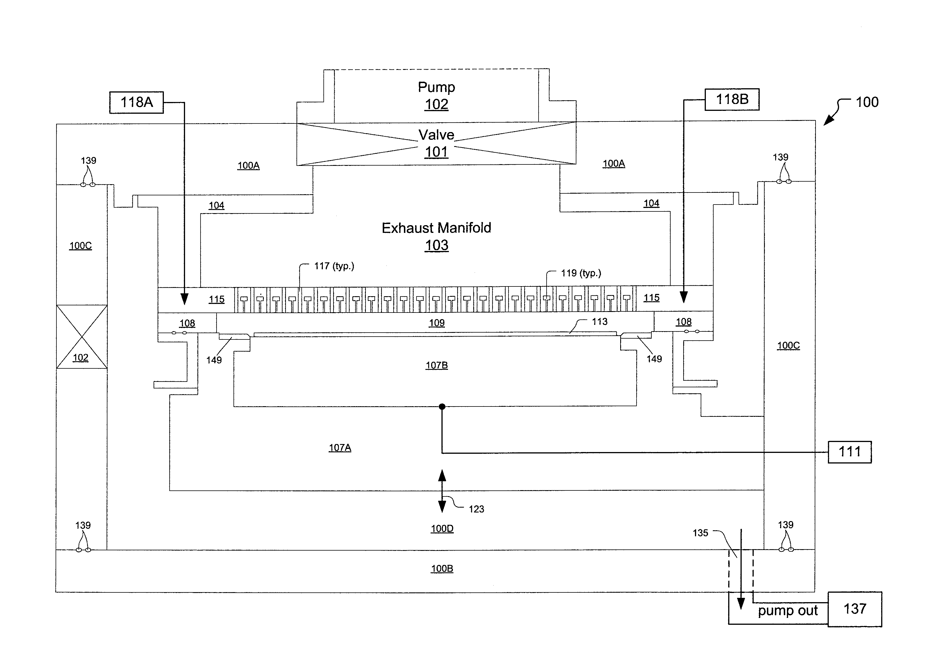
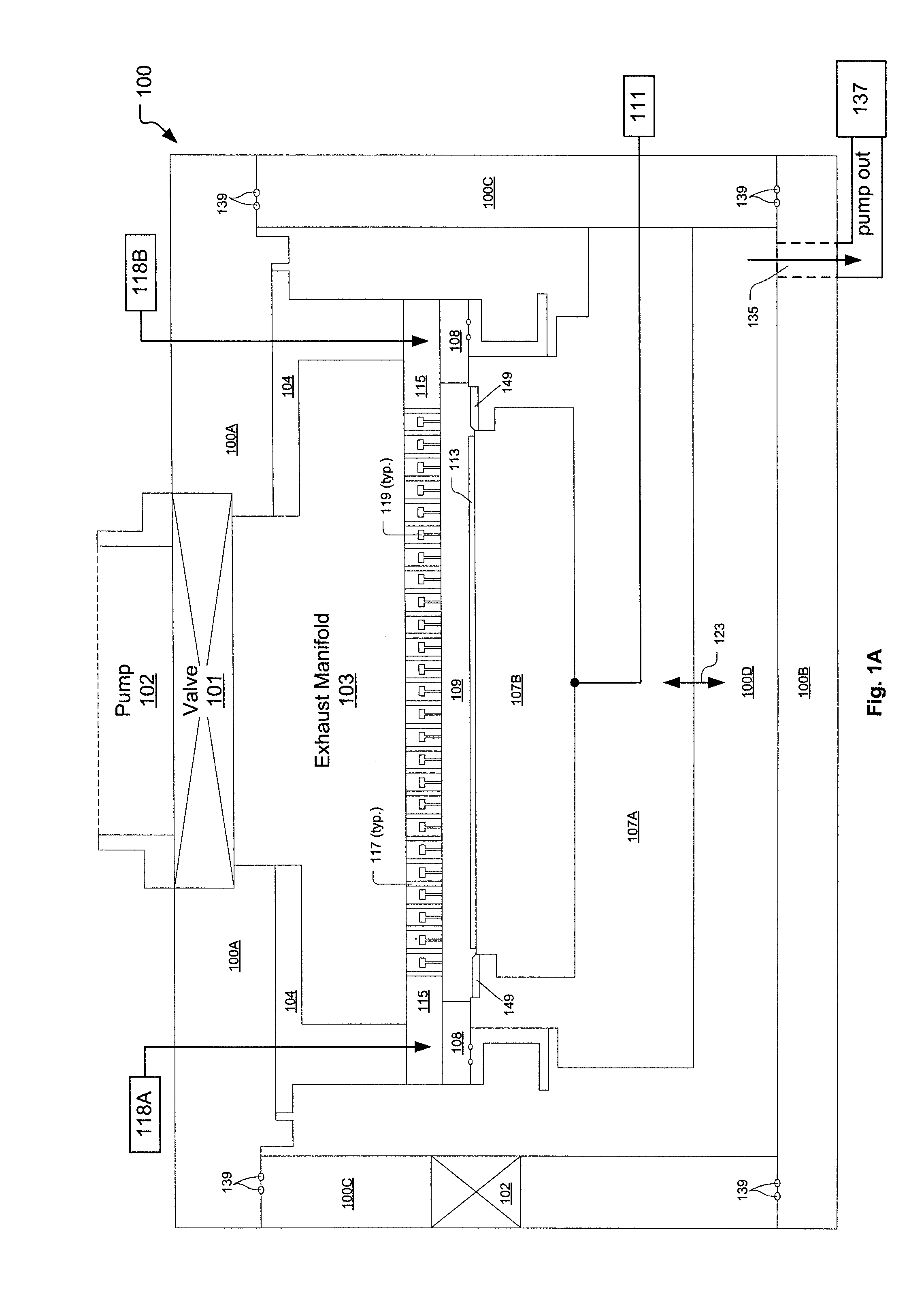
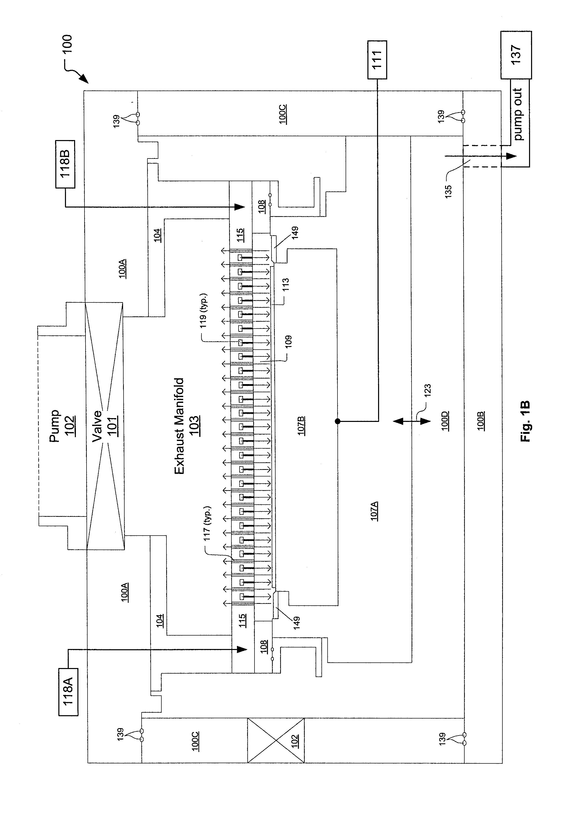
[0019]A semiconductor wafer processing apparatus is disclosed herein to enable precise control of plasma residence time and uniformity across a wafer to enable wafer fabrication processes that require rapid and uniform process gas injection and pump out. Examples of such wafer fabrication processes that require rapid and uniform process gas injection and pump out include, but are not limited to, atomic layer etching and atomic layer deposition.

[0020]The apparatus includes a gas distribution unit disposed above the plasma generation region, with the wafe...


PUM

PropertyMeasurementUnit
Forceaaaaaaaaaa
Flow rateaaaaaaaaaa
Densityaaaaaaaaaa

Abstract

An electrode is exposed to a plasma generation volume and is defined to transmit radiofrequency power to the plasma generation volume, and includes an upper surface for holding a substrate in exposure to the plasma generation volume. A gas distribution unit is disposed above the plasma generation volume and in a substantially parallel orientation to the electrode. The gas distribution unit includes an arrangement of gas supply ports for directing an input flow of a plasma process gas into the plasma generation volume in a direction substantially perpendicular to the upper surface of the electrode. The gas distribution unit also includes an arrangement of through-holes that each extend through the gas distribution unit to fluidly connect the plasma generation volume to an exhaust region. Each of the through-holes directs an exhaust flow from the plasma generation volume in a direction substantially perpendicular to the upper surface of the electrode.

Description

CROSS-REFERENCE TO RELATED APPLICATIONS[0001]This application is related to U.S. patent application Ser. No. ______ (Attorney Docket No. LAM2P690), filed on even date herewith, entitled “Dual Plasma Volume Processing Apparatus for Neutral / Ion Flux Control.” The disclosure of the above-identified related application is incorporated herein by reference in its entirety.BACKGROUND OF THE INVENTION[0002]As semiconductor feature sizes continue to get smaller, semiconductor fabrication processes struggle to keep pace. One type of fabrication process involves exposure of a semiconductor wafer to a plasma or other foam of reactant gas to either deposit material on the wafer or remove material from the wafer. Smaller feature sizes demand more accurate material deposition and etching control, which in turn requires more accurate control of how the wafer is exposed to the plasma / reactant gas. These more accurate control requirements may include more accurate control of plasma uniformity across ...

Claims


Application Information

Patent Timeline
IPC IPC(8): H01L21/3065C23C16/00H01L21/31
CPCC23C16/4412C23C16/45565C23C16/45574C23C16/45576H01L21/31H01J37/32091H01J37/32449H01J37/32834H01L21/3065C23C16/50C23C16/45563
Inventor DHINDSA, RAJINDERMARAKHATNOV, ALEXEIBAILEY, III, ANDREW D.
Owner LAM RES CORP
Why Eureka
Try Eureka