Line-width inspection device

a line-width inspection and inspection device technology, applied in the direction of instruments, television systems, material analysis, etc., can solve the problems of inability to accurately capture and define the edges of patterns, the deviation of the tolerable line-width in manufacturing processes, and the occurrence of shadows, so as to improve the precision of the image capture device

Inactive Publication Date: 2012-05-10
SHENZHEN CHINA STAR OPTOELECTRONICS TECH CO LTD
View PDF7 Cites 5 Cited by
  • Summary
  • Abstract
  • Description
  • Claims
  • Application Information

AI Technical Summary

Benefits of technology

[0006]A primary object of the invention is to provide a line-width inspection device which increases side light sources to compensate a shadow part of a pattern under inspection for insufficient illumination, so as to enhance precision of an image capturing device thereof that performs image capturing on the pattern under inspection.

Problems solved by technology

However, with the decrease in dimensions of semiconductors, tolerable line-width deviation in manufacturing processes is getting smaller.
Therefore, the line-width inspection technology still has following problems in practical use: since the light source device 90 vertically projects on the pattern under inspection in a radial manner, such that edges of the pattern 92 under inspection may not be lighted by the light source device 90 due to a thickness, and lead to an occurrence of shadows.
When being converted into grayscale values, the shadows will be an oblique line in a curve diagram, which means the edges of the pattern cannot be accurately captured and defined due to the interference of the shadows.
Hence, the occurrences of shadows will affect precision of image capturing and cause line-width inspection error.

Method used


Image

  • Line-width inspection device
  • Line-width inspection device
  • Line-width inspection device

Examples


Embodiment Construction

[0024]The foregoing objects, features and advantages adopted by the present invention can be best understood by referring to the following detailed description of the preferred embodiments and the accompanying drawings. Furthermore, the directional terms described in the present invention, such as upper, lower, front, rear, left, right, inner, outer, side and etc., are only directions referring to the accompanying drawings, so that the used directional terms are used to describe and understand the present invention, but the present invention is not limited thereto.

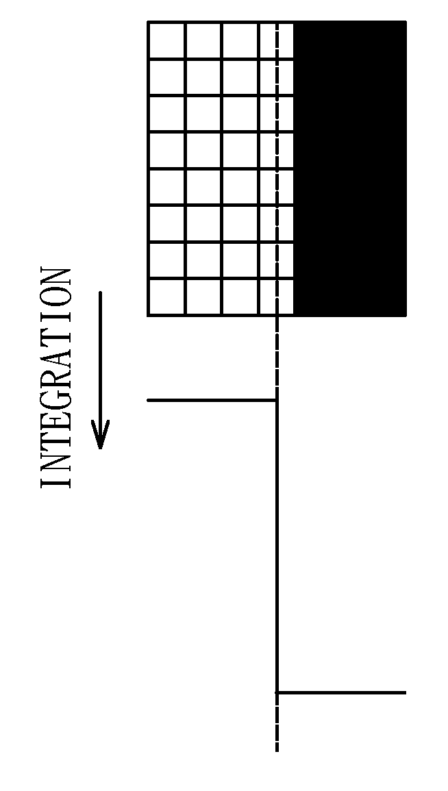
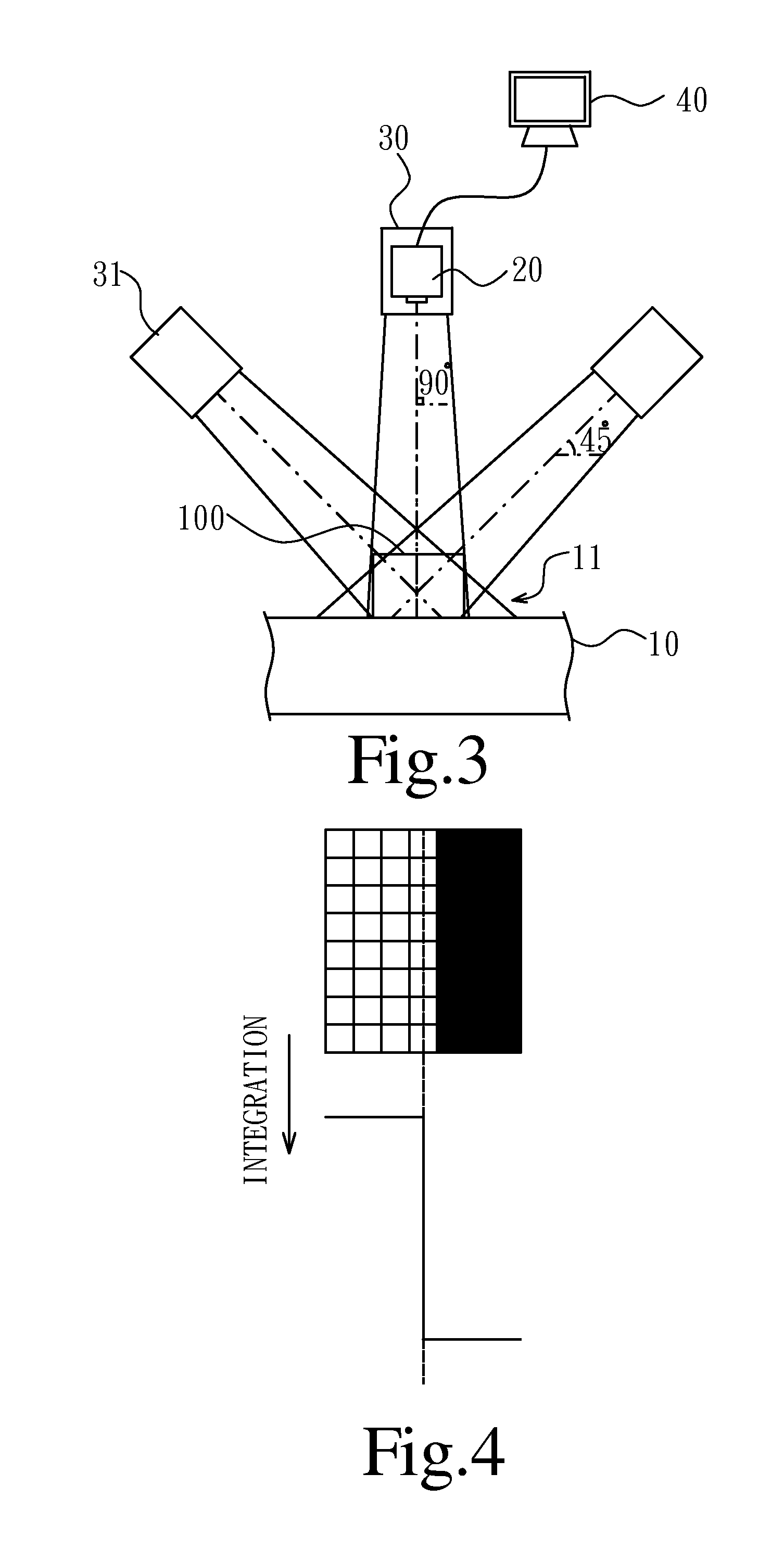
[0025]With reference to FIG. 3, FIG. 3 is a schematic view of a line-width inspection device according to a first embodiment of the present invention. The line-width inspection device comprises a platform 10, an image capturing device 20, a main light source device 30 and the at least one compensation light source device 31.

[0026]The platform 10 has an inspection area 11, and a surface of the platform 10 is provided for an...


PUM


Abstract

The present invention discloses a line-width inspection device. The line-width inspection device has a platform, an image capturing device, a main light source device and at least one compensation light source device. The image capturing device is mounted above the platform, aligned with an inspection area of the platform and captures images of a pattern under inspection in the inspection area. The main light source device is disposed above the platform and correspondingly provides forward illumination to the inspection area, and an incident direction thereof is perpendicular to the platform. The at least one compensation light source device is mounted above the platform and provides compensation illumination to the inspection area. The additional compensation light source device can prevent edges of the pattern under inspection from occurring shadows and affecting image capturing, so as to enhance precision of image capturing.

Description

FIELD OF THE INVENTION[0001]The present invention relates to a line-width inspection device, and more particularly to a line-width inspection device that increases compensation light sources to prevent from occurring shadows at edges of patterns under inspection and affecting image capturing.BACKGROUND OF THE INVENTION[0002]With the development of semiconductor manufacturing process, integrated circuit elements are progressively made much smaller. Therefore, in the semiconductor manufacturing process, control of critical dimension, such as line width, line pitch, etc. of fine circuit patterns on masks or wafers, is an important key point. Generally, manufacturers use line-width inspection device to inspect critical dimensions of circuit patterns, the line-width inspection device can be used to inspect if the line width or pitch is precise without deviation.[0003]With reference to FIG. 1, FIG. 1 is a schematic view of performing line-width inspection according to a conventional techn...

Claims


Application Information

Patent Timeline
Patent Type & Authority Applications(United States)
IPC IPC(8): H04N7/18
CPCG01N21/956
Inventor HE, CHENGMINGLIN, YUNG-YU
Owner SHENZHEN CHINA STAR OPTOELECTRONICS TECH CO LTD
Why Eureka
Try Eureka