Light emitting device and illumination apparatus using same
a technology of light emitting devices and illumination apparatus, which is applied in the direction of electrical apparatus, semiconductor/solid-state device manufacturing, and semiconductor devices. it can solve the problems of complex wiring structure, increased manufacturing cost, and difficult to efficiently dissipate heat from leds through the substrate, so as to simplify the wiring structure and efficiently dissipate heat from the solid light emitting elemen
- Summary
- Abstract
- Description
- Claims
- Application Information
AI Technical Summary
Benefits of technology
Problems solved by technology
Method used
Image

Examples
first embodiment
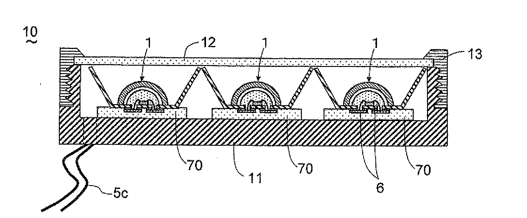
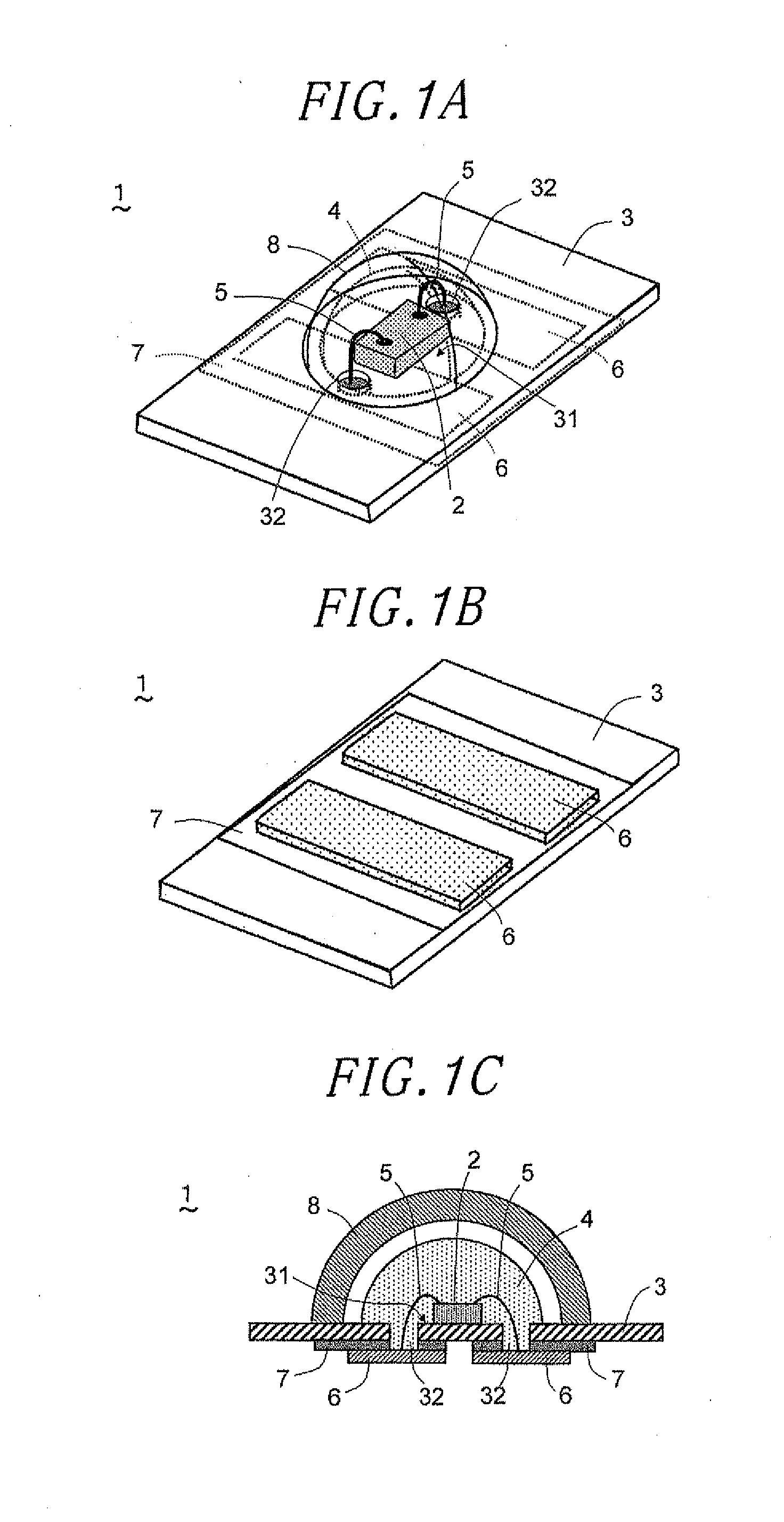
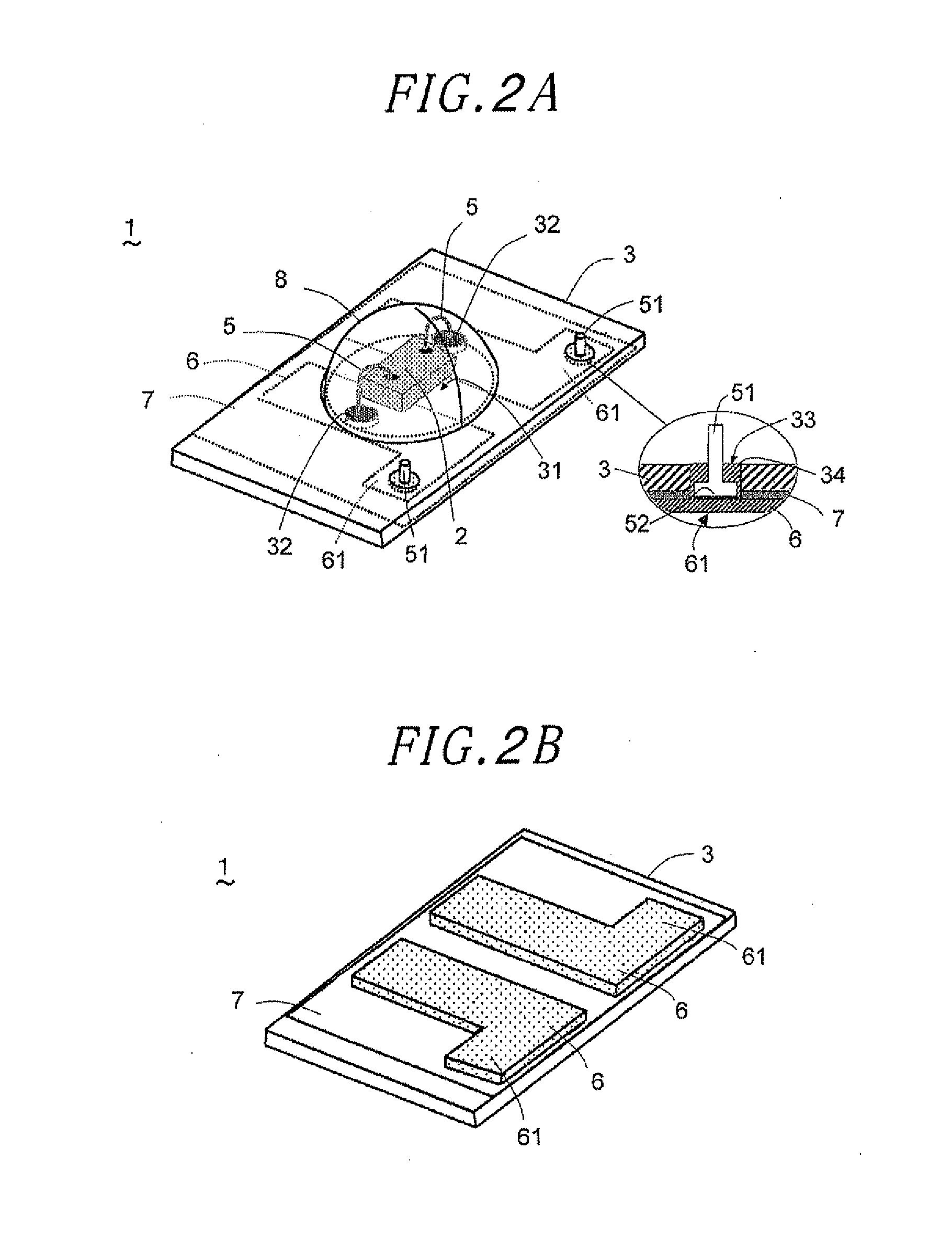
[0040]A light emitting device in accordance with the present invention will now be described with reference to FIGS. 1A through 1C. The light emitting device 1 of the present embodiment includes a light emitting diode (hereinafter referred to as “LED”) 2, i.e., a solid light emitting element serving as a light source, and a mounting substrate (hereinafter referred to as “substrate”) 3 to which the LED 2 is mounted. The light emitting device further includes an encapsulating member 4 for covering the LED 2 and lead frames 6 electrically connected to the LED 2 by means of wires 5. The lead frames 6 are arranged on the rear surface of the substrate 3. The substrate 3 has a front mounting surface 31 mounted with the LED 2 and provided with a smooth surface region covered with the encapsulating member 4, and wire holes 32 through which the wires 5 are inserted from the front mounting surface 31 of the substrate 3 to the rear surface thereof.
[0041]The lead frames 6 are bonded and fixed to...
eighth embodiment
[0073]Next, a light emitting device in accordance with the present invention will be described with reference to FIGS. 11A and 115. In the light emitting device 1 of the present embodiment, the extension portions 37 have peripheral portions 37a that are bent to the side of the LEDs 2. The peripheral portions 37a are bent at, e.g., about 45 degrees, with respect to the mounting surface 31. Just like the mounting surface 31, the peripheral portions 37a are subjected to high reflection treatment.
[0074]In the light emitting device 1 employing a single LED 2, the peripheral portions 37a may be provided to surround either all sides or only two sides of the LED 2 and the wavelength converting member 8. In this case, other configurations remain the same as those of the first embodiment. In the light emitting device 1 employing a plurality of LEDs 2 arranged along a line, the peripheral portions 37a are arranged along the opposite sides of the row of the LEDs 2. In this case, the light emitt...
seventh embodiment
[0075]With this configuration, there is provided the same effects as in the In addition, the light emitted from the LEDs 2 is reflected by the peripheral portions 37a and is projected forward in the optical axis direction of the light emitting device 1. This helps increase the light projecting efficiency of an illuminating device equipped with the light emitting device 1.
PUM
 Abstract
Description
Claims
Application Information
 - R&D Engineer
- R&D Manager
- IP Professional
- Industry Leading Data Capabilities
- Powerful AI technology
- Patent DNA Extraction
Browse by: Latest US Patents, China's latest patents, Technical Efficacy Thesaurus, Application Domain, Technology Topic.
© 2024 PatSnap. All rights reserved.Legal|Privacy policy|Modern Slavery Act Transparency Statement|Sitemap