
Non-volatile memory device and method for fabricating the same

Inactive Publication Date: 2012-07-05
SK HYNIX INC
View PDF1 Cites 27 Cited by
  • Summary
  • Abstract
  • Description
  • Claims
  • Application Information

AI Technical Summary

Benefits of technology

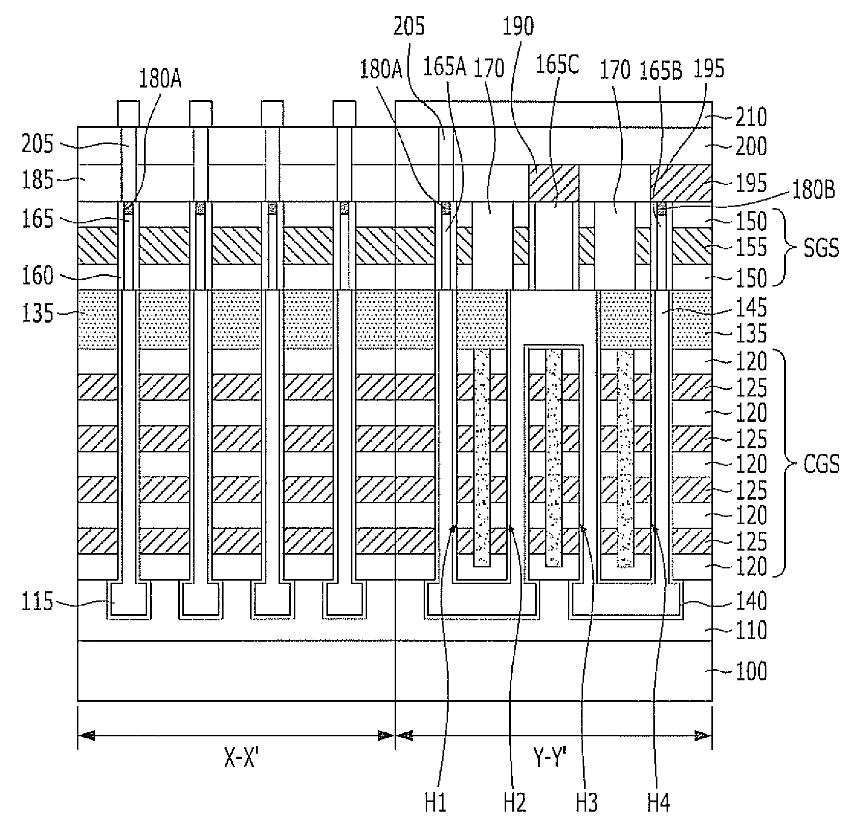
[0015]In accordance with yet another exemplary embodiment of the present invention a method for fabricating a non-volatile memory device includes: forming a first conductive layer over a substrate, selectively etching the first conductive layer to form two or more grooves, forming a first sacrificial layer pattern to fill the two or more grooves, forming a cell gate structure by stacking a first inter-layer dielectric layer, a second conductive layer, and another first inter-layer dielectric layer, forming a first channel hole, a second channel hole, a third channel hole, and a fourth channel hole, wherein the first channel hole and the second channel hole expose the first sacrificial layer pattern in one of the grooves, and the third channel hole and fourth channel hole expose the first sacrifi

Problems solved by technology

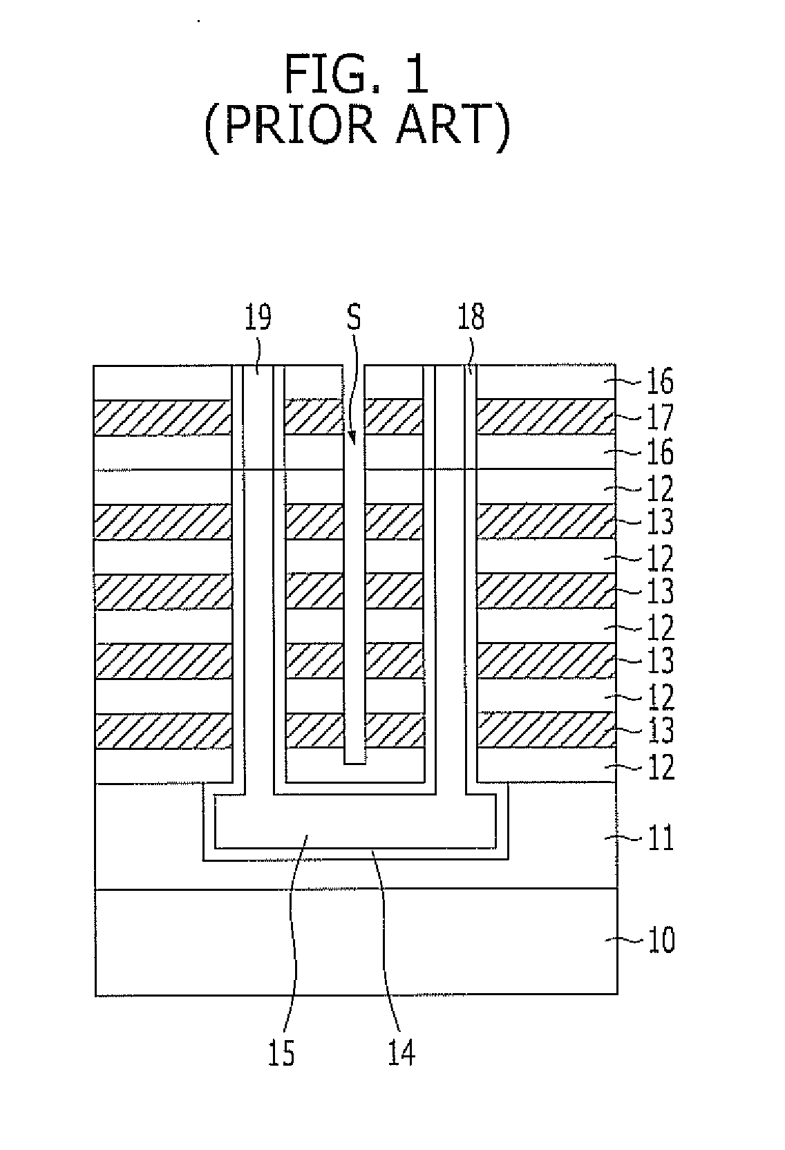
Therefore, it is impossible to perform a data erase operation by applying an erase voltage to a substrate body in the known three-dimensional non-volatile memory device of FIG. 1, and instead, the known three-dimensional non-volatile memory device performs an erase operation by supplying holes based on a Gate-Induced Drain Leakage (GIDL) effect.
However, when an erase operation is performed based on the GIDL effect, the erase rate may decrease because holes are not sufficiently supplied.

Method used


Image

  • Non-volatile memory device and method for fabricating the same
  • Non-volatile memory device and method for fabricating the same
  • Non-volatile memory device and method for fabricating the same

Examples


Embodiment Construction

[0018]Exemplary embodiments of the present invention will be described below in more detail with reference to the accompanying drawings. The present invention may, however, be embodied in different forms and should not be construed as limited to the embodiments set forth herein. Rather, these embodiments are provided so that this disclosure will be thorough and complete, and will fully convey the scope of the present invention to those skilled in the art. Throughout the disclosure, like reference numerals refer to like parts throughout the various figures and embodiments of the present invention.

[0019]The drawings are not necessarily to scale and in some instances, proportions may have been exaggerated in order to clearly illustrate features of the embodiments. When a first layer is referred to as being “on” a second layer or “on” a substrate, it not only refers to a case where the first layer is formed directly on the second layer or the substrate, but also a case where a third lay...


PUM


Abstract

A non-volatile memory device including a memory string including a plurality of memory cells coupled in series. The non-volatile memory device includes the memory string including a first semiconductor layer and a second conductive layer with a memory gate insulation layer therebetween, a first selection transistor comprising a second semiconductor layer coupled with one end of the first semiconductor layer, a second selection transistor comprising a third semiconductor layer coupled with the other end of the first semiconductor layer, and a fourth semiconductor layer contacting the first semiconductor layer in a region where the second conductive layer is not disposed.

Description

CROSS-REFERENCE TO RELATED APPLICATIONS[0001]The present application claims priority of Korean Patent Application No. 10-2010-0138837, filed on Dec. 30, 2010, which is incorporated herein by reference in its entirety.BACKGROUND OF THE INVENTION[0002]Exemplary embodiments of the present invention relate to a non-volatile memory device and a fabrication method thereof, and more particularly, to a non-volatile memory device having a three-dimensional (3D) structure where memory cells are formed along channels protruding perpendicular to a substrate, and a method for fabricating the same.[0003]A non-volatile memory device retains data stored therein although a power source is cut off. At present, diverse non-volatile memory devices, such as flash memory, are widely used.[0004]As the improvement in the integration degree of a two-dimensional memory device which is fabricated in a single layer over a silicon substrate reaches limitations, a three-dimensional non-volatile memory device whi...

Claims


Application Information

Patent Timeline
IPC IPC(8): H01L27/092H01L21/336
CPCH01L27/11582H01L27/11565H10B43/10H10B43/27H01L21/823871H01L21/823885H01L29/7926
Inventor LEE, SANG-BUM
Owner SK HYNIX INC
Learn More