Methods of fabricating bipolar transistor for improved isolation, passivation and critical dimension control

a bipolar transistor and passivation technology, applied in the field of semiconductor devices and processing, can solve the problems of reducing the thickness of the transistor, reducing the service life of the transistor, and reducing the use of the transistor which eventually results from the fabrication process

Inactive Publication Date: 2012-07-12
INT BUSINESS MASCH CORP
View PDF25 Cites 0 Cited by
  • Summary
  • Abstract
  • Description
  • Claims
  • Application Information

AI Technical Summary

Benefits of technology

[0007]According to one aspect of the invention, a first dielectric spacer formed on a sidewall of a dummy emitter mandrel is removed after a raised extrinsic base layer and covering dielectric layer are formed. Thereafter, the dummy emitter mandrel as well as the first dielectric spacer are removed, after which a second dielectric spacer is formed within the opening that results. As a result, the second dielectric spacer, which is not subjected to RIE processing, provides a desired level of isolation and passivation to the bipolar transistor at tighter dimensions than that which could be achieved through the technique described above as background. In a particular embodiment, an additional layer of silicon nitride is disposed over the oxide etch stop layer as a sacrificial layer which protects the oxide etch stop layer from being reduced in thickness and / or being undercut during the RIE process and one or more cleaning processes conducted after the RIE process.

Problems solved by technology

As a result, the spacer may become eroded during the RIE process.
These undesirable after-effects of the RIE process are generally more pronounced when the oxide layer is a deposited oxide layer than when it is a thermally grown layer.
After experiencing the level of damage shown in FIG. 3B, the transistor which eventually results from the fabrication process becomes unusable.
Such undercutting can make the final transistor inoperative.
Summarizing, the spacer and oxide etch stop layer according to the prior art can be eroded and damaged to a point where they no longer serve their intended functions of isolating the emitter from the raised extrinsic base and protecting the intrinsic base layer from damage.

Method used


Image

  • Methods of fabricating bipolar transistor for improved isolation, passivation and critical dimension control
  • Methods of fabricating bipolar transistor for improved isolation, passivation and critical dimension control
  • Methods of fabricating bipolar transistor for improved isolation, passivation and critical dimension control

Examples


Embodiment Construction

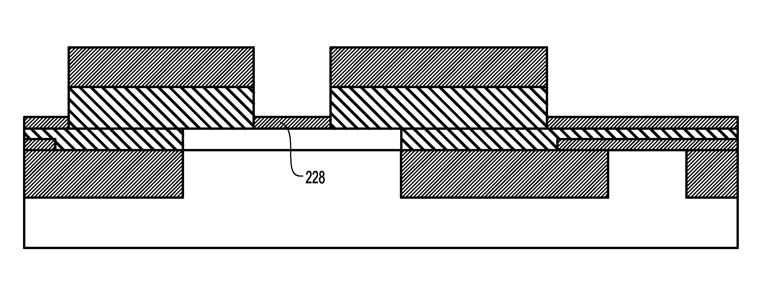
[0014]Accordingly, methods are provided herein which address the above-described difficulties faced by the processing described above in the background. In the embodiments of the invention described herein, a first dielectric spacer which is formed on a sidewall of a dummy emitter mandrel is removed after the raised extrinsic base layer and covering dielectric layer are formed. Thereafter, a second dielectric spacer is formed within the opening that results. In other words, the first spacer is used as a replaceable or disposable spacer to protect the sidewalls of the raised extrinsic base layer and covering dielectric layer during the removal of the dummy emitter mandrel. The second dielectric spacer, not being subjected to damage from RIE processing, therefore, provides a desired level of isolation between the raised extrinsic base and the emitter and tighter emitter final critical dimension control than that which could be achieved through the technique described above as backgrou...


PUM


Abstract

A first (e.g. replaceable or disposable) dielectric spacer formed on a sidewall of a dummy emitter mandrel is removed after a raised extrinsic base layer and covering dielectric layer are formed. Thereafter, a second dielectric spacer is formed within the opening that results. As a result, the second dielectric spacer, which is not subjected to RIE processing, provides a desired level of isolation and tighter emitter final critical dimension than that which could be achieved through the technique described in the prior art. In a particular embodiment, an additional layer of silicon nitride is disposed over a passivation oxide layer as a sacrificial layer which protects the passivation oxide layer from being reduced in thickness and / or being undercut during the RIE process and one or more cleaning processes conducted after the RIE process.

Description

CROSS-REFERENCE TO RELATED APPLICATION[0001]This application is a divisional of currently co-pending U.S. patent application Ser. No. 11 / 161,286, filed on Jul. 28, 2005, the subject matter of which is incorporated herein by reference in its entirety.BACKGROUND OF THE INVENTION[0002]The present invention relates to semiconductor devices and processing.[0003]FIG. 1 illustrates a known method of forming a bipolar transistor having a raised extrinsic base self-aligned to an emitter of the transistor. As shown in FIG. 1, a mandrel 10 is formed in a location to be occupied by the emitter, the mandrel thus being a “dummy emitter” mandrel. The mandrel includes an etch stop layer, which is typically a sacrificial oxide layer 11, over which a lower layer of polysilicon 12 and an upper layer of silicon nitride 14 are disposed. The oxide etch stop layer can either be thermally grown as a silicon dioxide layer from the semiconductor material present at the interface to the intrinsic base layer 1...

Claims


Application Information

Patent Timeline
Patent Type & Authority Applications(United States)
IPC IPC(8): H01L29/73
CPCH01L29/7378H01L29/66242
Inventor KHATER, MARWAN H.
Owner INT BUSINESS MASCH CORP
Why Eureka
Try Eureka