Wafer processing method

a processing method and wafer technology, applied in the field of wafer processing method, can solve the problems of inability to accurately divide the wafer along the streets, the focal point of the laser beam cannot be set at a proper position, and the wafer cannot be warped, so as to prevent the occurrence of chipping on the wafer, reduce the thickness, and increase the holding force of the adhesive resin for attaching the wafer to the rigid plate

Active Publication Date: 2010-12-09
DISCO CORP
View PDF0 Cites 16 Cited by
  • Summary
  • Abstract
  • Description
  • Claims
  • Application Information

AI Technical Summary

Benefits of technology

[0007]It is therefore an object of the present invention to provide a wafer processing method which can accurately divide the wafer along the streets and can reduce the thickness of each device divided from the wafer.
[0012]According to the present invention, the wafer can be divided accurately along the streets without the influence of warpage of the wafer reduced in thickness.
[0013]Further, the holding force of the adhesive resin for attaching the wafer to the rigid plate is increased by performing the holding force increasing step before the back grinding step. Accordingly, the wafer can be reliably held through the adhesive resin to the rigid plate in the back grinding step, so that the movement of the wafer can be prevented to thereby prevent the occurrence of chipping on the wafer.
[0014]Further, the rigid plate attaching step includes the steps of filling each groove formed on the front side of the rigid plate with the water permeable layer and next attaching the front side of the wafer through the adhesive resin to the front side of the rigid plate. In the holding force decreasing step, the hot water is introduced through the water permeable layer to the adhesive resin, so that the adhesive resin is effectively swelled by the hot water to thereby decrease the holding force of the adhesive resin. Accordingly, the rigid plate can be easily removed from the front side of the wafer in the rigid plate removing step.

Problems solved by technology

In the case of grinding the back side of a wafer formed from a sapphire substrate or a silicon carbide substrate to reduce the thickness of the wafer to about 50 μm by using a grinding apparatus before forming the laser processed grooves along the streets on the front side of the wafer, so as to improve the characteristics of each optical device, there is a possibility of warpage of the wafer.
As a result, the focal point of the laser beam cannot be set at a proper position and the wafer cannot therefore be divided accurately along the streets.

Method used


Image

  • Wafer processing method
  • Wafer processing method
  • Wafer processing method

Examples


Embodiment Construction

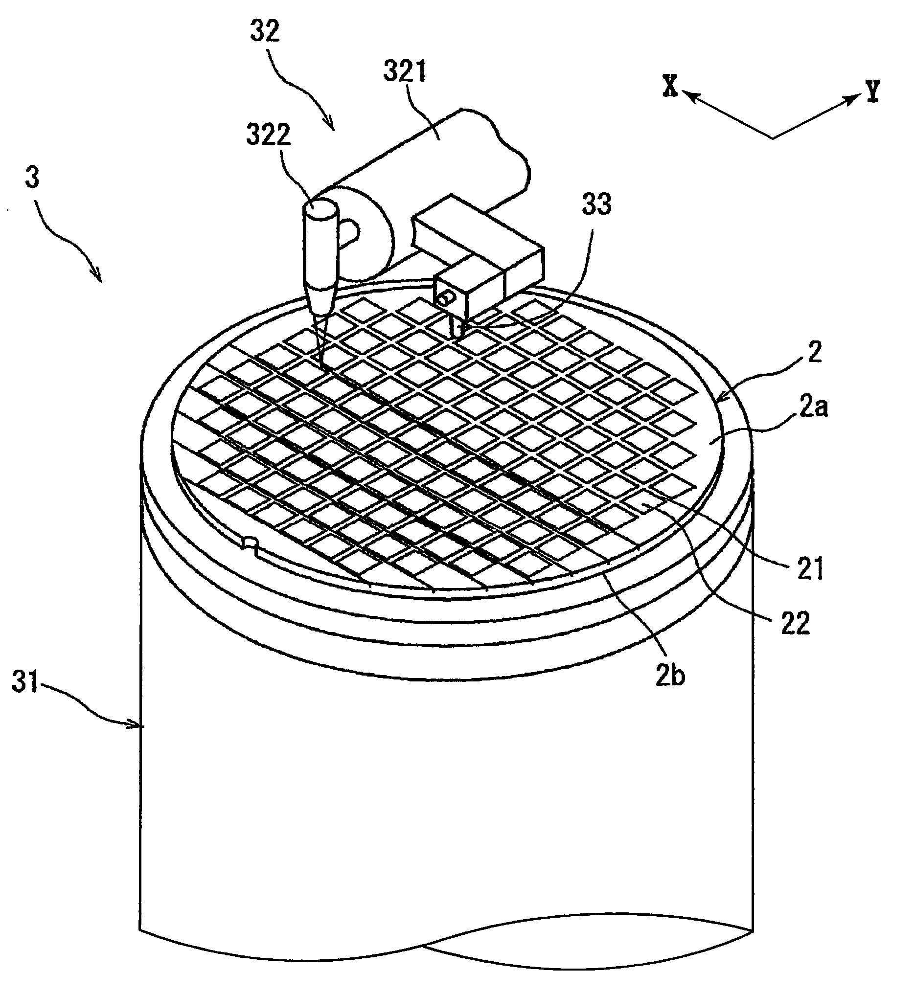
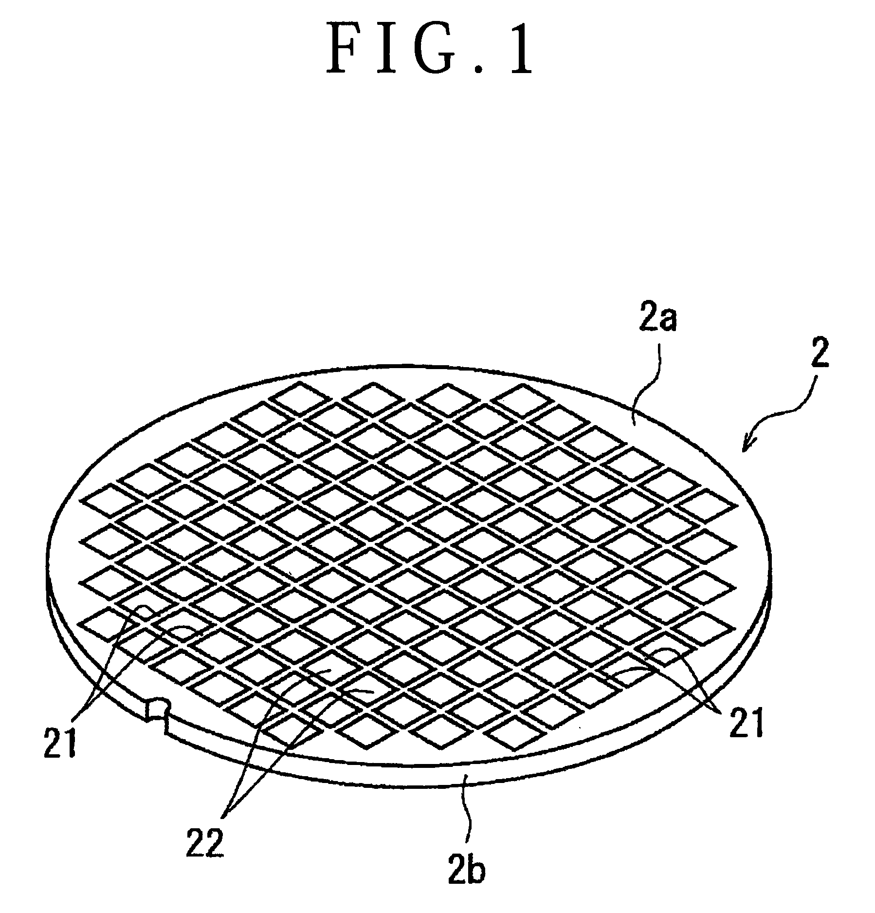
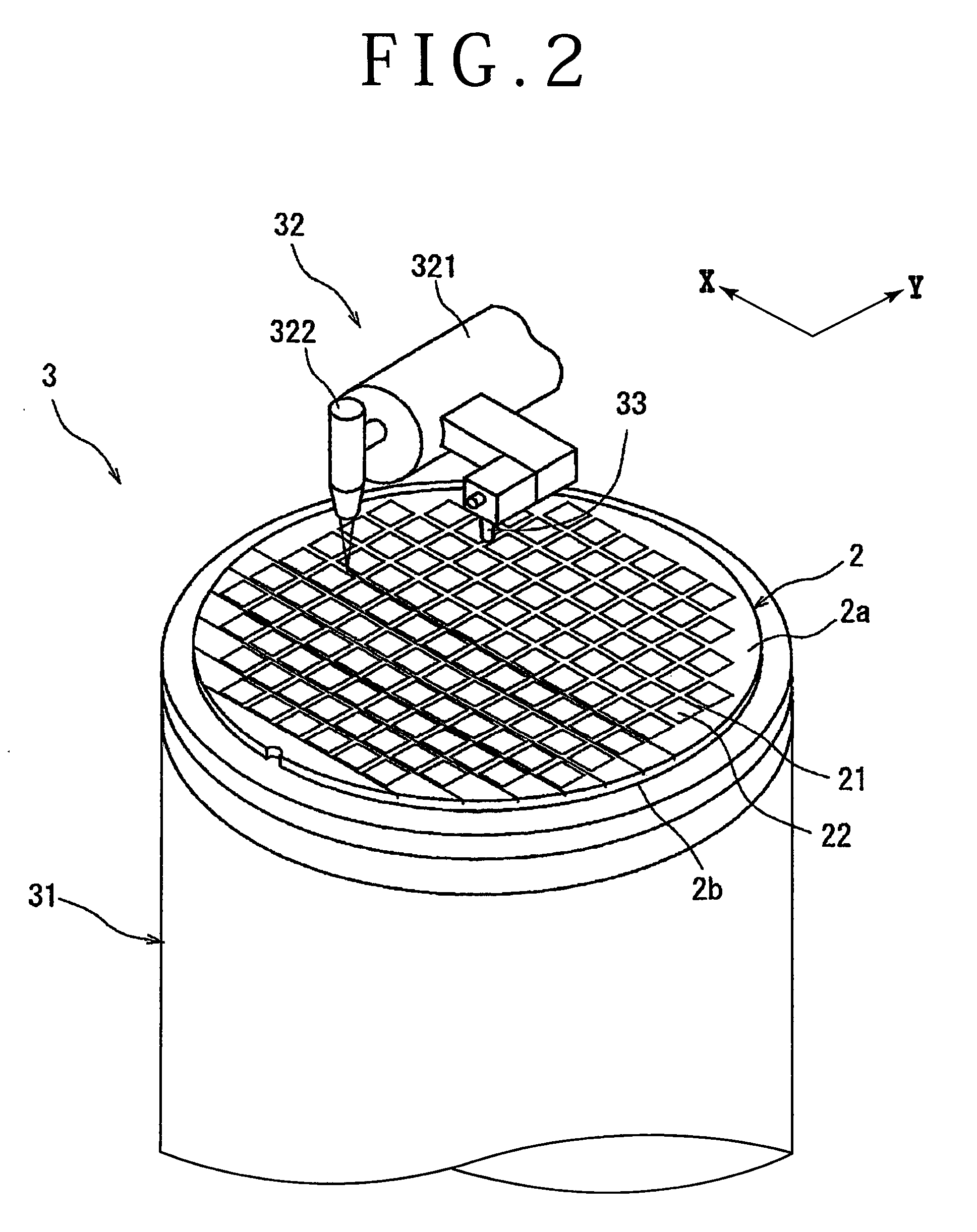
[0029]A preferred embodiment of the wafer processing method according to the present invention will now be described in detail with reference to the attached drawings. FIG. 1 is a perspective view of an optical device wafer 2 as a wafer. The optical device wafer 2 shown in FIG. 1 is formed from a sapphire wafer having a thickness of 600 μm, for example. The optical device wafer 2 has a front side 2a and a back side 2b. A plurality of crossing streets 21 are formed on the front side 2a of the optical device wafer 2 to thereby partition a plurality of rectangular regions where a plurality of optical devices 22 such as light emitting diodes and laser diodes are respectively formed. These optical devices 22 are formed by laminating gallium nitride compound semiconductors or the like. There will now be described a wafer processing method for dividing the optical device wafer 2 into the individual optical devices 22 along the streets 21.

[0030]In the wafer processing method according to th...


PUM

PropertyMeasurementUnit
depthaaaaaaaaaa
depthaaaaaaaaaa
widthaaaaaaaaaa

Abstract

A wafer processing method for dividing a wafer into individual devices along streets. The wafer processing method includes the steps of forming a division groove on the front side of the wafer along each street, attaching the front side of the wafer to the front side of a rigid plate having a plurality of grooves by using an adhesive resin, applying ultraviolet radiation to the adhesive resin to thereby increase the holding force of the adhesive resin, grinding the back side of the wafer to expose the division grooves to the back side of the wafer, attaching an adhesive tape to the back side of the wafer, immersing the wafer and the rigid plate in hot water to swell the adhesive resin, thereby decreasing the holding force of the adhesive resin, and removing the rigid plate from the front side of the wafer.

Description

BACKGROUND OF THE INVENTION[0001]1. Field of the Invention[0002]The present invention relates to a wafer processing method for dividing a wafer into individual devices along a plurality of crossing streets formed on the front side of the wafer, the individual devices being respectively formed in a plurality of regions partitioned by the streets.[0003]2. Description of the Related Art[0004]In a semiconductor device fabrication process, a plurality of crossing division lines called streets are formed on the front side of a substantially disk-shaped semiconductor wafer to thereby partition a plurality of regions where devices such as ICs and LSIs are respectively formed. The semiconductor wafer is cut along the streets to thereby divide the regions where the devices are formed from each other, thus obtaining the individual devices. Further, an optical device wafer is formed by laminating gallium nitride compound semiconductors or the like on a sapphire substrate or a silicon carbide su...

Claims


Application Information

Patent Timeline
Patent Type & Authority Applications(United States)
IPC IPC(8): H01L21/78
CPCB23K26/367H01L21/78B23K26/4075B23K26/364B23K26/40B23K2103/50
Inventor SEKIYA, KAZUMA
Owner DISCO CORP
Why Eureka
Try Eureka