
Liquid crystal panel and pixel structure thereof

a liquid crystal display and pixel technology, applied in semiconductor devices, electrical devices, instruments, etc., can solve problems such as light leakage in dark states

Active Publication Date: 2012-09-20
HANNSTAR DISPLAY CORPORATION
View PDF21 Cites 7 Cited by
  • Summary
  • Abstract
  • Description
  • Claims
  • Application Information

AI Technical Summary

Benefits of technology

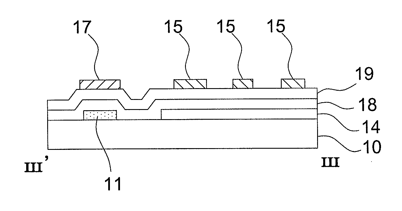
The present patent provides a liquid crystal panel and pixel structure that solves the light leakage problem in horizontal electric field type liquid crystal displays. It also improves the contrast of the display. The panel includes a transparent substrate, gate and data lines, switching transistors, electrodes, and a shield layer. The shield layer overlaps with the gate lines and is electrically isolated from the electrodes. The panel can be used in in-plane or fringe field switching mode liquid crystal displays. The technical effect of the patent is to reduce the impact of stray electric fields on the orientation of liquid crystals and improve the display quality of horizontal electric field type liquid crystal displays.

Problems solved by technology

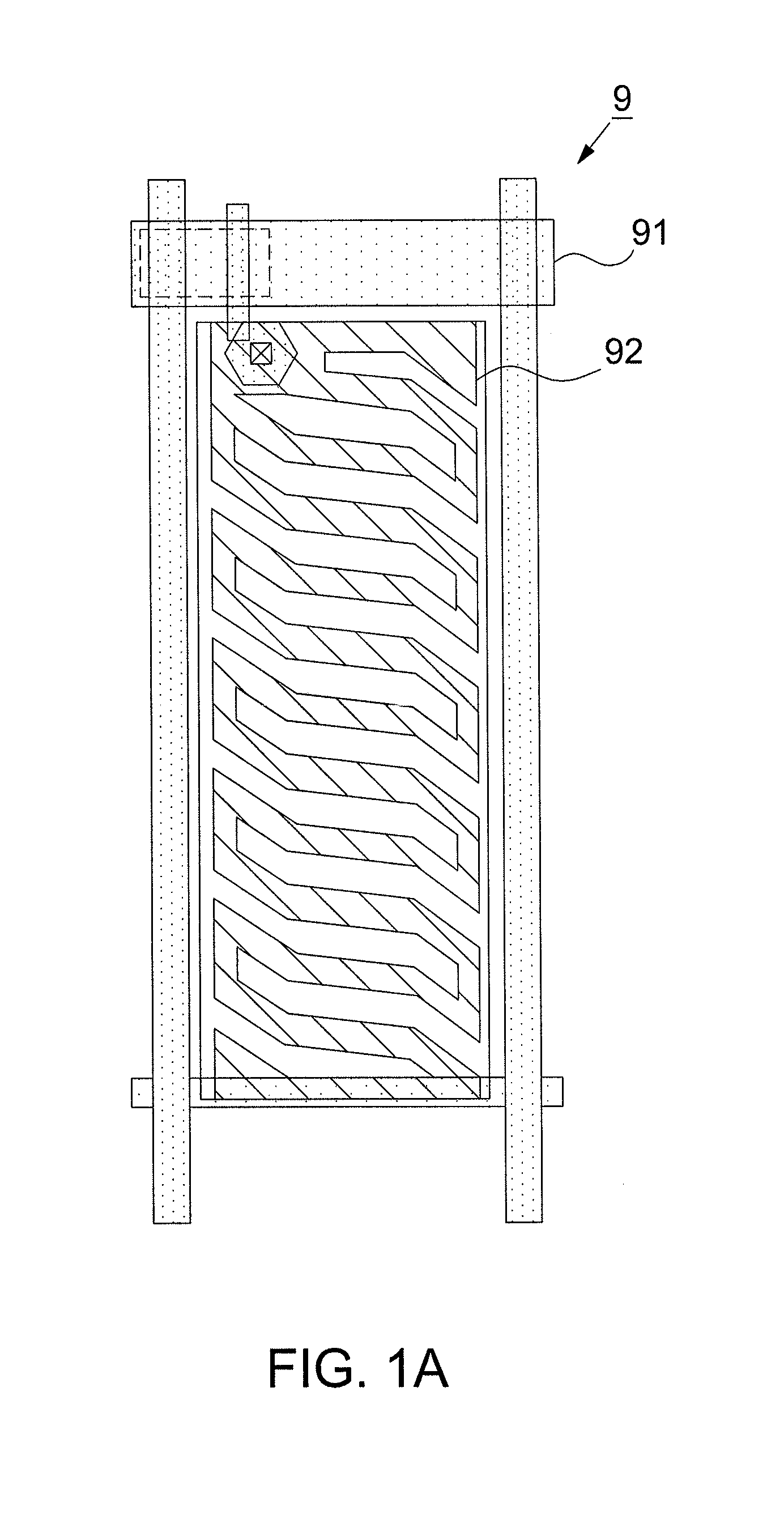
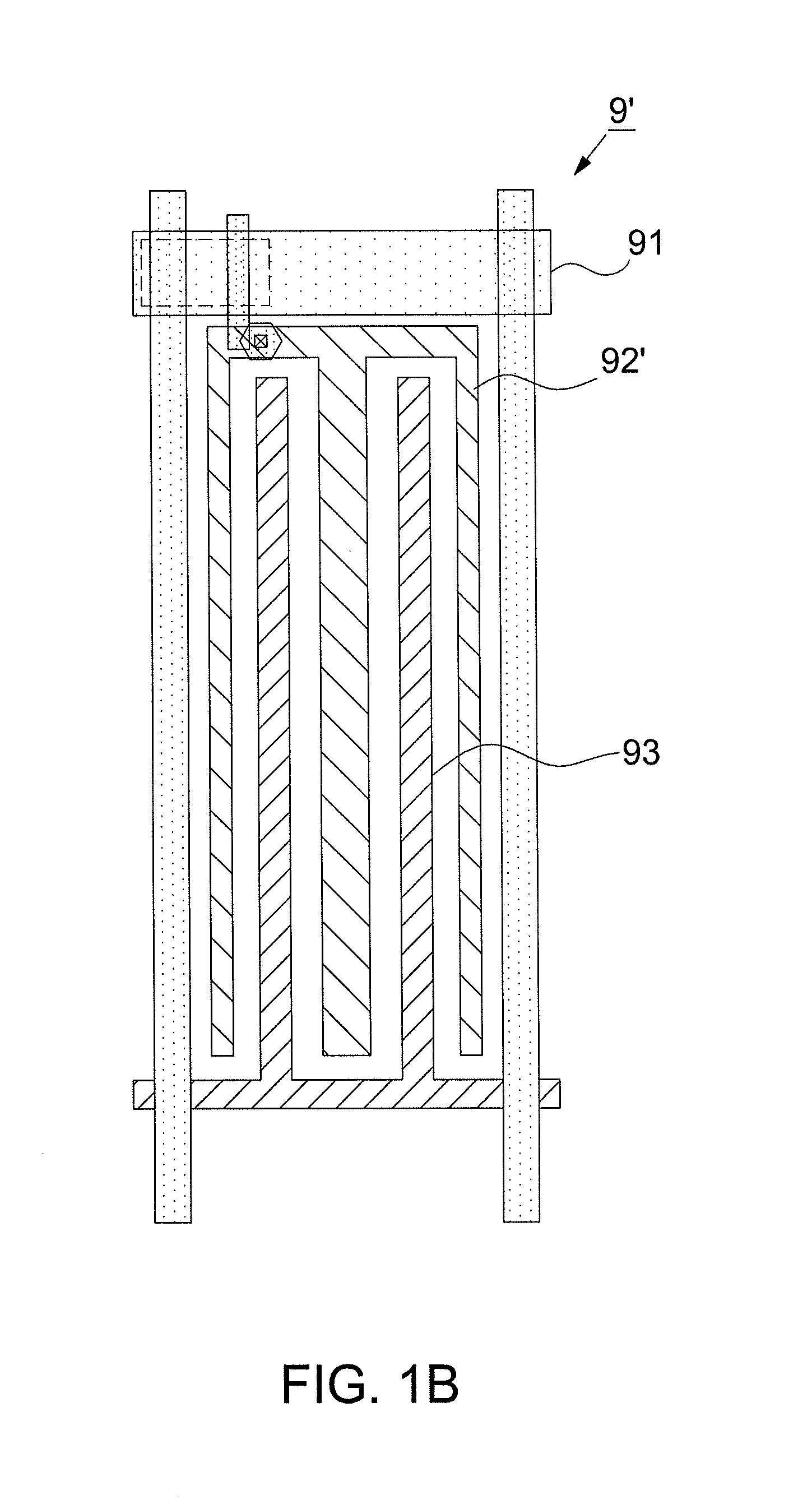
However, in horizontal electric field type liquid crystal display electric charges can gradually accumulate in the stray capacitance between gate lines and other components of the display with the pixel operation to generate stray electric field which can influence the distribution of the transverse electric field during the pixel operation such that the orientation of liquid crystal molecules close to the gate lines can deviate from the desired direction to cause light leakage in dark state.

Method used


Image

  • Liquid crystal panel and pixel structure thereof
  • Liquid crystal panel and pixel structure thereof
  • Liquid crystal panel and pixel structure thereof

Examples


Embodiment Construction

[0021]It should be noted that, wherever possible, the same reference numbers will be used throughout the drawings to refer to the same or like parts.

[0022]In the drawings of the present disclosure, only a part of the components are shown and other components that are not directly related to the present disclosure are omitted.

[0023]The liquid crystal panel and pixel structure thereof of the present disclosure will be illustrated by means of a fringe field switching (FFS) mode liquid crystal panel.

[0024]Please refer to FIG. 2, it shows a schematic plan view of a pixel structure of the FFS mode liquid crystal panel according to an embodiment of the present disclosure. Since the color filter substrate is well known to the art, the pixel structure shown in FIG. 2 only includes the pixel structure of the array substrate not including that of the color filter substrate.

[0025]The pixel structure 1 includes a transparent substrate, and two scan lines 11 and 11′, two data lines 12 and 12′, a ...


PUM


Abstract

There is provided a pixel structure of a liquid crystal panel including a transparent substrate, and a gate line, a data line, a switching transistor, a first electrode, a second electrode and a shield layer formed on the transparent substrate. The gate line is substantially perpendicular to the data line. The switching transistor is located adjacent to a crossing point of the gate line and the data line, and is configured to input a display voltage of the data line to the second electrode according to the control of the gate line. The first electrode and the second electrode are arranged in such a way that the display voltage forms a transverse electric field between the first electrode and the second electrode. The shield layer overlaps at least a part of the gate and is electrically isolated from the first electrode and the second electrode.

Description

CROSS REFERENCE TO RELATED APPLICATION[0001]This application claims the priority benefit of Taiwan Patent Application Serial Number 100108882, filed on Mar. 16, 2011, the full disclosure of which is incorporated herein by reference.BACKGROUND[0002]1. Field of the Invention[0003]This invention generally relates to a liquid crystal display device and, more particularly, to a horizontal electric field type liquid crystal display and pixel structure thereof.[0004]2. Description of the Related Art[0005]Liquid crystal display technologies can be divided into two categories: twisted nematic liquid crystal displays (TN-LCD) and horizontal electric field type liquid crystal displays, wherein the horizontal electric field type liquid crystal displays further include in-plan switching (IPS) mode liquid crystal displays and fringe field switching (FFS) mode liquid crystal displays. In TN-LCD, liquid crystal molecules rotate following the variation of a longitudinal electric field between two op...

Claims


Application Information

Patent Timeline
Patent Type & Authority Applications(United States)
IPC IPC(8): H01L33/08
CPCH01L27/124G02F2001/136218G02F1/134363G02F1/136218
Inventor YU, CHIA HUAWANG, I FANGKUO, FENG WEEILAI, JUI CHIJEN, KO RUAYCHAO, GUANG SHIUNG
Owner HANNSTAR DISPLAY CORPORATION
Learn More