Miniature Wafer-Level Camera Modules

a technology of camera modules and wafers, applied in the field of camera modules, can solve the problems of inability to benefit from the economies of scale and potential cost savings associated with wafer-level manufacturing processes, and the process used for conventional camera modules tends to impose certain limits on the size and/or manufacturing cost achievable for these conventional camera modules

Inactive Publication Date: 2012-09-27
OMNIVISION TECH INC
View PDF4 Cites 38 Cited by
  • Summary
  • Abstract
  • Description
  • Claims
  • Application Information

AI Technical Summary

Problems solved by technology

This manufacturing process has certain drawbacks for certain implementations.
In particular, the manufacturing process used for conventional camera modules tends to impose certain limits on the size and / or manufacturing cost achievable for these conventional camera modules.
Moreover, conventional manufacturing processes are not able to benefit from the economies of scale and potential cost savings associated with wafer-level manufacturing processes.

Method used


Image

  • Miniature Wafer-Level Camera Modules
  • Miniature Wafer-Level Camera Modules
  • Miniature Wafer-Level Camera Modules

Examples


Embodiment Construction

[0015]In the following description, numerous specific details are set forth. However, it is understood that embodiments of the invention may be practiced without these specific details. In other instances, well-known circuits, structures and techniques have not been shown in detail in order not to obscure the understanding of this description.

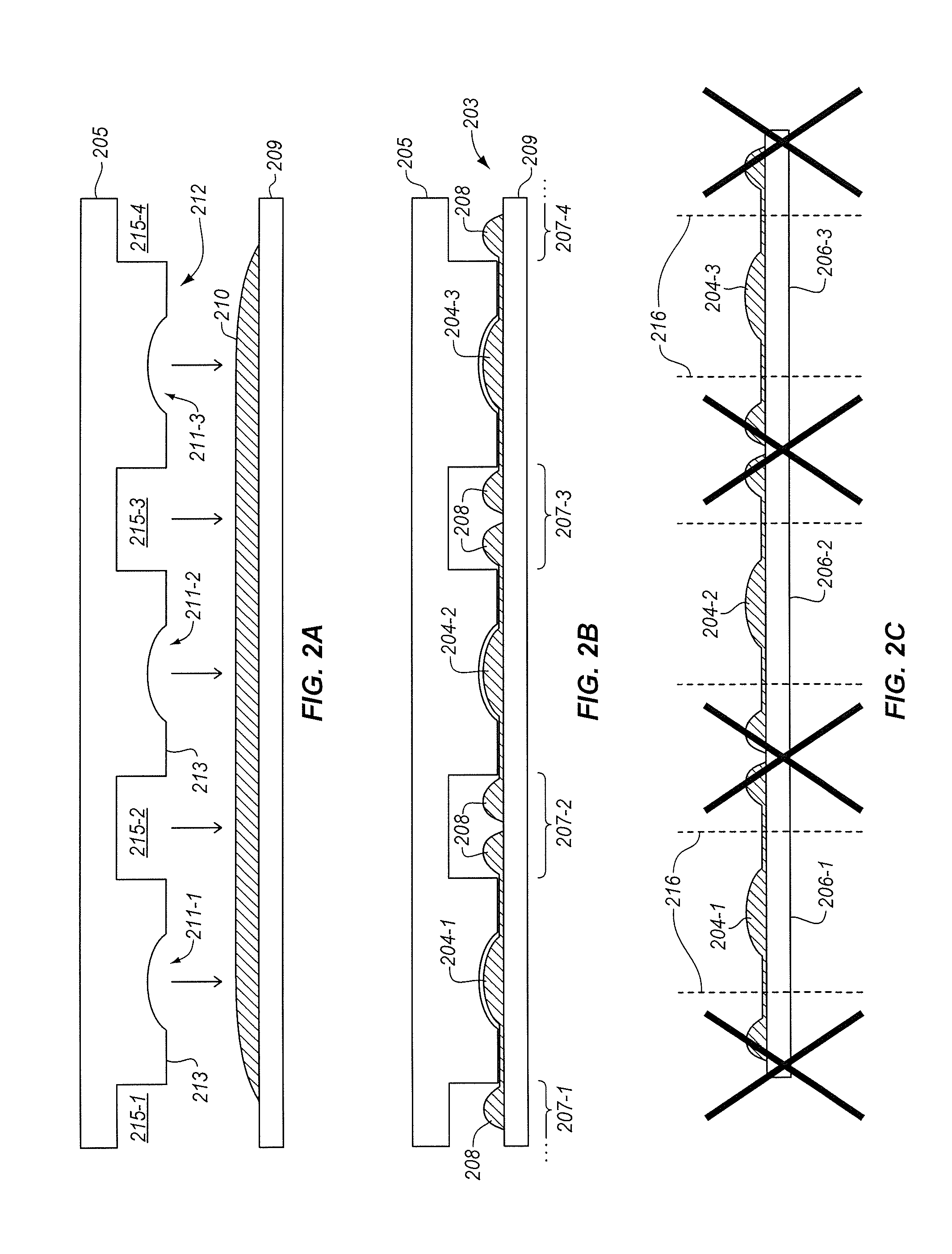
[0016]Wafer-level camera modules provide an alternative to conventional camera modules and can be manufactured at sizes and / or manufacturing costs below those typically achievable for conventional camera modules. As the name suggests, wafer-level camera modules may be manufactured by a process that incorporates one or more wafer-level manufacturing operations. As in conventional camera module manufacture, the image sensor arrays are typically manufactured in parallel, at the wafer-level. However, in contrast to conventional camera module manufacture, the lenses used for wafer-level camera modules are also commonly manufactured at the wafer-leve...


PUM

PropertyMeasurementUnit
field of viewaaaaaaaaaa
distanceaaaaaaaaaa

Abstract

In one aspect, a method includes providing a lens substrate having an array of lenses. The lens substrate includes an overflow region next to each lens of the array. Each overflow region includes an overflow lens material. The method also includes separating the lens substrate into a plurality of smaller lens substrates. Each of the smaller lens substrates has one of the single lens and the plurality of stacked lenses. Separating the lens substrate into the smaller lens substrates may include removing or substantially removing the overflow regions. In one aspect, the method may be performed as a method of making a miniature camera module. Other methods are also described, as are miniature camera modules.

Description

BACKGROUND[0001]1. Field[0002]Embodiments of the invention pertain to camera modules or to methods of manufacturing camera modules. In particular, embodiments of the invention pertain to miniature wafer-level camera modules or to methods of manufacturing miniature wafer-level camera modules.[0003]2. Background Information[0004]A representative manufacturing process for conventional camera modules may include manufacturing individual lenses one at a time or in small groups, but not through a wafer-level manufacturing process. In conventional camera modules, the individual lenses are assembled and attached to individual image sensor arrays. For example, one or more individual lenses may be assembled with a lens barrel or other lens holder, the lens barrel or holder may be assembled with a lens mount, and the lens mount may be mounted on a printed circuit board or flex substrate on which the individual image sensor array has been mounted. Other individual components such as filters, re...

Claims


Application Information

Patent Timeline
Patent Type & Authority Applications(United States)
IPC IPC(8): H04N5/225B32B38/04B26D3/00H04N7/18
CPCB26F1/38B29D11/00298H04N5/2251Y10T29/53H04N2005/2255Y10T156/1052H04N5/2257Y10T83/04H01L27/14625H01L27/14636H01L27/14643H01L27/14685H01L27/14698B29D11/00307H04N23/555H04N23/55H04N23/57H04N23/54
Inventor KUBALA, KENNETHSILVEIRA, PAULO E. X.TACHIHARA, SATORU
Owner OMNIVISION TECH INC
Why Eureka
Try Eureka