Compatible vertical double diffused metal oxide semiconductor transistor and lateral double diffused metal oxide semiconductor transistor and manufacture method thereof

a metal oxide semiconductor and lateral double-diffused technology, applied in the direction of transistors, semiconductor devices, electrical appliances, etc., can solve the problems of not being able to arrange compatibly ldmos and vertical double-diffused metal oxide semiconductors (vdmos), and achieve the effect of accommodating a performance demand

Active Publication Date: 2012-10-11
CSMC TECH FAB2 CO LTD
View PDF0 Cites 9 Cited by
  • Summary
  • Abstract
  • Description
  • Claims
  • Application Information

AI Technical Summary

Benefits of technology

[0021]As compared with the prior art, the invention has such an advantage that the NSINK area is formed in the epitaxial layer between the isolation area and the adjacent gate in the VDMOS transistor area, and the NSINK area is communicated with the N-buried layer area, which enables communication between the drains, thereby achieving compatibility of an LDMOS transistor with a VDMOS transistor on a BCD process platform and further accommodating a performance demand for high voltage and large current.

Problems solved by technology

However since the high voltage MOS transistors in the existing BCD process are primarily LDMOS, there is no possibility to arrange compatibly LDMOS and Vertical Double-diffused Metal Oxide Semiconductor (VDMOS) on the same process platform to accommodate the high voltage-resistance of the LDMOS and the large current driving capability of the VDMOS.

Method used


Image

  • Compatible vertical double diffused metal oxide semiconductor transistor and lateral double diffused metal oxide semiconductor transistor and manufacture method thereof
  • Compatible vertical double diffused metal oxide semiconductor transistor and lateral double diffused metal oxide semiconductor transistor and manufacture method thereof
  • Compatible vertical double diffused metal oxide semiconductor transistor and lateral double diffused metal oxide semiconductor transistor and manufacture method thereof

Examples


Embodiment Construction

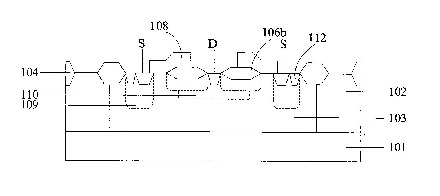
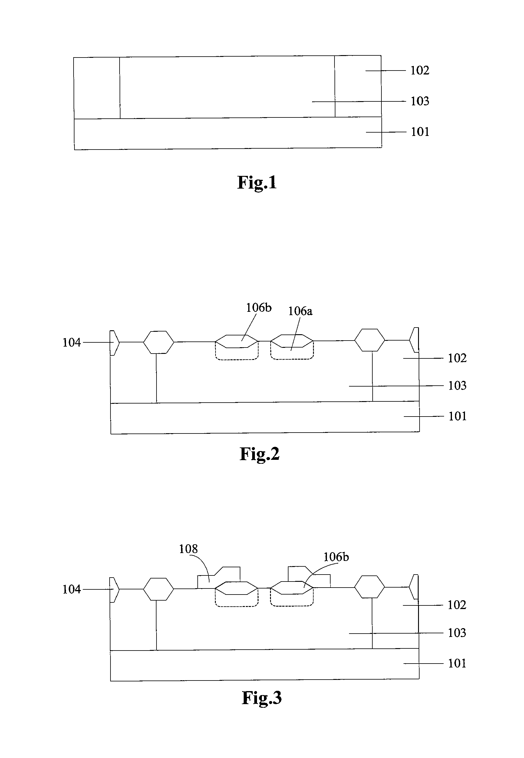
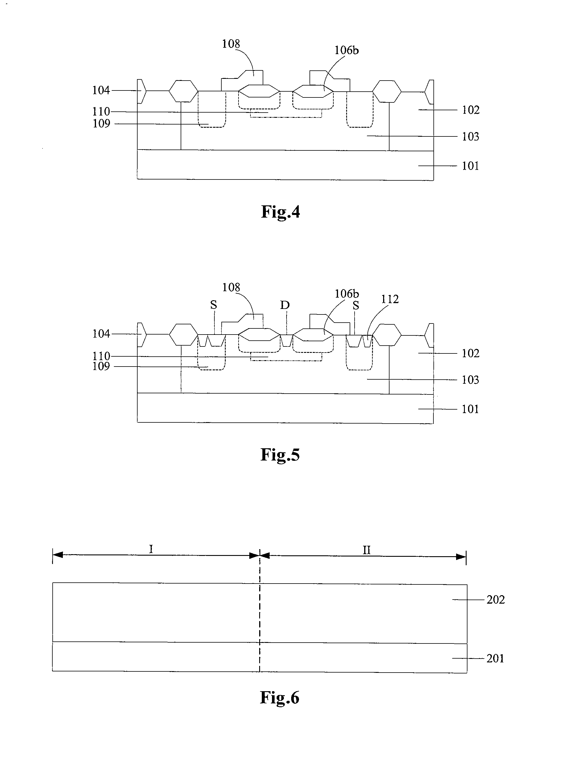
[0024]In an embodiment of the invention in which an LDMOS transistor compatible with a VDMOS transistor is fabricated, a substrate is prepared with an LDMOS transistor area and a VDMOS transistor area; ions are injected into the substrate to form an N-buried layer area; an epitaxial layer is formed in the N-buried layer area, and then ions are injected into the epitaxial layer to form an N-well and a P-well in the LDMOS transistor area and a high voltage N-well in the VDMOS transistor area; an isolation area is formed at the interface between the N-well and the P-well in the LDMOS transistor area and at the interface between the LDMOS transistor area and the VDMOS transistor area; a drift area is formed in the area of the P-well of the LDMOS transistor area; a gate is formed on a part of the epitaxial layer and a part of the drift area in the area of the P-well of the LDMOS transistor area, and in the VDMOS transistor area; a PBODY area is formed in the epitaxial layer between the g...


PUM


Abstract

A method for manufacturing compatible vertical double diffused metal oxide semiconductor (VDMOS) transistor and lateral double diffused metal oxide semiconductor (LDMOS) transistor includes: providing a substrate having an LDMOS transistor region and a VDMOS transistor region; forming an N-buried region in the substrate; forming an epitaxial layer on the N-buried layer region; forming isolation regions in the LDMOS transistor region and the VDMOS transistor region; forming a drift region in the LDMOS transistor region; forming gates in the LDMOS transistor region and the VDMOS transistor region; forming PBODY regions in the LDMOS transistor region and the VDMOS transistor region; forming an N-type GRADE region in the LDMOS transistor region; forming an NSINK region in the VDMOS transistor region, where the NSINK region is in contact with the N-buried layer region; forming sources and drains in the LDMOS transistor region and the VDMOS transistor region; and forming a P+ region in the LDMOS transistor region, where the P+ region is in contact with the source.

Description

[0001]This application claims the priority to Chinese Patent Application no. 200910209187.5, filed with the Chinese Patent Office on Oct. 28, 2009 and entitled “LDMOS TRANSISTOR COMPATIBLE WITH VDMOS TRANSISTOR AND METHOD FOR FABRICATING THE SAME”, which is hereby incorporated by reference in its entirety.FIELD OF THE INVENTION[0002]The present invention relates to the field of fabricating a semiconductor device and in particular to an LDMOS transistor compatible with a VDMOS transistor and a method for fabricating the same.BACKGROUND OF THE PRESENT INVENTION[0003]Along with constant development of semiconductor processes, the three originally independent branches of BIPOLAR, Complementary Metal Oxide Semiconductor (CMOS) and Double-diffused Metal Oxide Semiconductor (DMOS) field effect transistors have been integrated constantly with each other so that the processes of BICMOS into which the BIPOLAR and the CMOS are integrated together and of BCD into which the three are integrated ...

Claims


Application Information

Patent Timeline
Patent Type & Authority Applications(United States)
IPC IPC(8): H01L29/78H01L21/8238
CPCH01L21/823418H01L21/823487H01L27/088H01L29/0847H01L21/8249H01L29/66659H01L29/66712H01L29/7809H01L29/7835H01L29/42368
Inventor GUI, LINCHUNWANG, LEZHAO, ZHIYONGHE, LILI
Owner CSMC TECH FAB2 CO LTD
Why Eureka
Try Eureka