Electronic device including acoustic waveguide

a technology of acoustic waveguide and electronic device, which is applied in the direction of transducer casing/cabinet/support, substation equipment, electric transducers, etc., can solve the problems of deteriorating voice call quality of electronic devices, difficult to secure a path for such sensors, and difficult to secure an acoustic path connected to the receiver, etc., to achieve enhanced call quality and improve sound quality

Pending Publication Date: 2021-08-05
SAMSUNG ELECTRONICS CO LTD
View PDF4 Cites 1 Cited by
  • Summary
  • Abstract
  • Description
  • Claims
  • Application Information

AI Technical Summary

Benefits of technology

[0011]According to various embodiments, the electronic device may deliver improved sound quality in a voice call by including a plurality of acoustic waveguides between an acoustic hole provided as a receiver and a speaker outputting the sound of a received call. In one embodiment, another additional device or electronic component may obtain a path for receiving or obtaining various pieces of information from the outside of the electronic device or outputting optical signals through a space or area between the acoustic waveguides. For example, according to various embodiments, the electronic device may have other electronic components easily placed therein and may deliver enhanced call quality by providing a plurality of acoustic waveguides in a voice call.

Problems solved by technology

However, in the reality of designing or manufacturing the entire front surface of an electronic device as an active area of the display in order to provide improved image quality, for example, a larger screen and a high-definition image, it may be difficult for such sensors to secure a path through which various pieces of information may be received or acquired.
However, it may be difficult to secure an acoustic path connected to the receiver because other additional devices are disposed inside the upper end of the electronic device, as mentioned above.
For example, the voice call quality of the electronic device may deteriorate.

Method used


Image

  • Electronic device including acoustic waveguide
  • Electronic device including acoustic waveguide
  • Electronic device including acoustic waveguide

Examples


Embodiment Construction

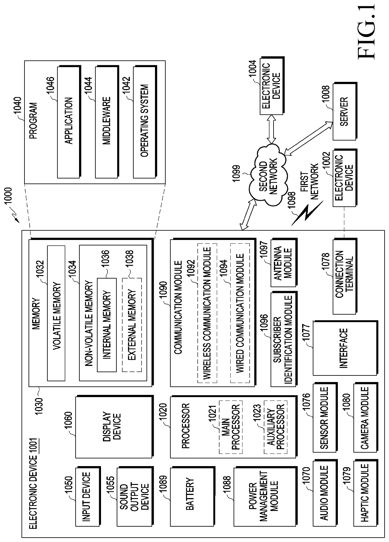
[0026]FIG. 1 is a block diagram illustrating an electronic device 1001 in a network environment 1000 according to various embodiments. Referring to FIG. 1, the electronic device 1001 in the network environment 1000 may communicate with an electronic device 1002 via a first network 1098 (e.g., a short-range wireless communication network), or an electronic device 1004 or a server 1008 via a second network 1099 (e.g., a long-range wireless communication network). According to an embodiment, the electronic device 1001 may communicate with the electronic device 1004 via the server 1008. According to an embodiment, the electronic device 1001 may include a processor 1020, memory 1030, an input device 1050, a sound output device 1055, a display device 1060, an audio module 1070, a sensor module 1076, an interface 1077, a haptic module 1079, a camera module 1080, a power management module 1088, a battery 1089, a communication module 1090, a subscriber identification module (SIM) 1096, or an...


PUM


Abstract

An electronic device is disclosed, including a housing including a first surface, a second surface facing away from the first surface, and a side surface structure at least partially surrounding a space formed between the first surface and the second surface, an acoustic hole formed in the housing and configured to emit a sound in a direction the first surface faces, a speaker disposed in the housing, and a first acoustic waveguide and a second acoustic waveguide together providing an acoustic path between the speaker and the acoustic hole, wherein the second acoustic waveguide is different from the first acoustic waveguide.

Description

CROSS-REFERENCE TO RELATED APPLICATION(S)[0001]This application is based on and claims priority under 35 U.S.C. 119 to Korean Patent Application No. 10-2020-0012542, filed on Feb. 3, 2020, in the Korean Intellectual Property Office, the disclosure of which is herein incorporated by reference in its entirety.BACKGROUNDTechnical Field[0002]Various embodiments of the disclosure relate to audio output in an electronic device, and more particularly, to an electronic device with acoustic waveguides for producing audio channels within the electronic device.Description of Related Art[0003]The development of electronic communication technology has produced the trend of integration, in which various functionalities are all included in a single electronic device. For example, smartphones include the functionalities of a media player, imaging device, and scheduler / organizers, as well as traditional communication functionality, and furthermore may implement additional functions by having any num...

Claims


Application Information

Patent Timeline
Patent Type & Authority Applications(United States)
IPC IPC(8): H04R1/28H04M1/03H04R1/34
CPCH04R1/2857H04R2499/11H04R1/345H04M1/035H04M1/026H04M1/0264H04M2250/12H04R1/323H04R1/1083H04R1/026H04R1/028
Inventor KIM, KIWONPARK, CHOONGHYOBAEK, INCHEOLSONG, JIHOONYANG, SEONGKWANJUN, SUNGSOOLEE, BYOUNGHEECHO, JOONRAEHWANG, HOCHUL
Owner SAMSUNG ELECTRONICS CO LTD
Why Eureka
Try Eureka