
Plated Through Hole Void Detection in Printed Circuit Boards by Detecting A pH-Sensitive Component

a technology of printed circuit boards and voids, which is applied in the direction of printed element electric connection formation, electrical apparatus casings/cabinets/drawers, instruments, etc., can solve the problems of difficult detection of defects, voids may form, and voids are known issues of plated through hole voids

Active Publication Date: 2013-01-17
IBM CORP
View PDF6 Cites 10 Cited by
  • Summary
  • Abstract
  • Description
  • Claims
  • Application Information

AI Technical Summary

Benefits of technology

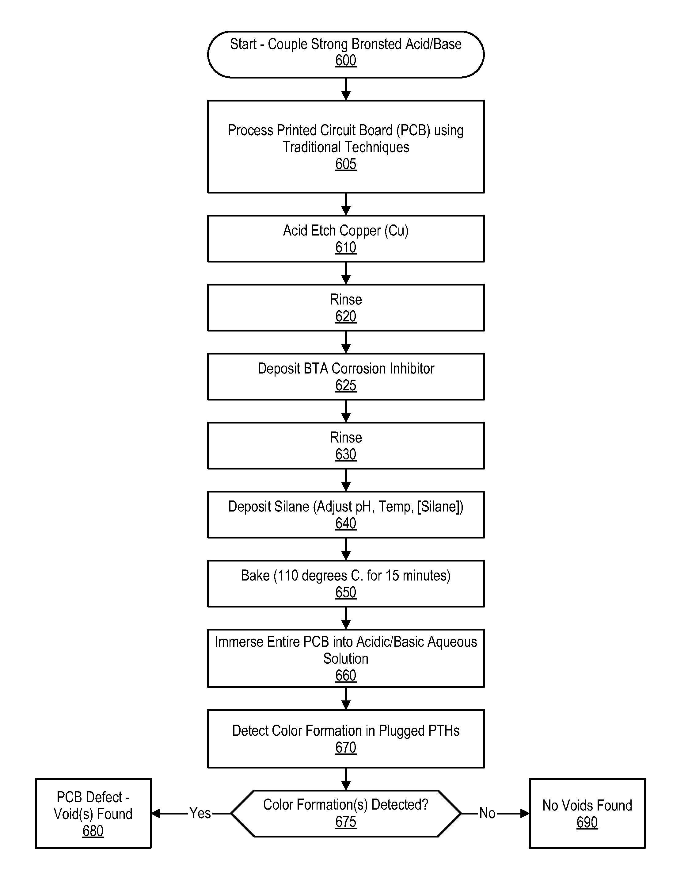
The patent text describes a method to detect defects in printed circuit boards using a pH-indicating compound. The compound is incorporated in one of the layers of the circuit board, and conductive pathways are formed on the surface of the board. When the board is exposed to a pH-activating solution, any plated-through hole defects can be easily identified by detecting a color formation at the surface location where the defect is located. This approach provides a reliable and efficient way to inspect printed circuit boards for quality control.

Problems solved by technology

Plated through hole voids are a known issue when manufacturing printed circuit boards (PCB).
Plated through hole voids may potentially cause failure during assembly and are also considered as a long term reliability issue of the printed circuit boards.
For example, voids may form if the copper plating solution was blocked by air bubbles, foreign material, or dry film resist residues.
This defect is difficult to detect using currently-available inspection capability or test equipment.
The voids may not entirely encircle the hole wall and thus may not result in an electrical open thereby making it difficult to detect by an electrical method.
In the subsequent card assembly and field application processes, these voids may become an intermittent open, or even a dead open, due to high thermal stress in the assembly process or temperature cycling during the application stage.

Method used


Image

  • Plated Through Hole Void Detection in Printed Circuit Boards by Detecting A pH-Sensitive Component
  • Plated Through Hole Void Detection in Printed Circuit Boards by Detecting A pH-Sensitive Component
  • Plated Through Hole Void Detection in Printed Circuit Boards by Detecting A pH-Sensitive Component

Examples


Embodiment Construction

[0013]The terminology used herein is for the purpose of describing particular embodiments only and is not intended to be limiting of the invention. As used herein, the singular forms “a”, “an” and “the” are intended to include the plural forms as well, unless the context clearly indicates otherwise. It will be further understood that the terms “comprises” and / or “comprising,” when used in this specification, specify the presence of stated features, integers, steps, operations, elements, and / or components, but do not preclude the presence or addition of one or more other features, integers, steps, operations, elements, components, and / or groups thereof.

[0014]The corresponding structures, materials, acts, and equivalents of all means or step plus function elements in the claims below are intended to include any structure, material, or act for performing the function in combination with other claimed elements as specifically claimed. The description of the present invention has been pr...


PUM

PropertyMeasurementUnit
pHaaaaaaaaaa
pH-sensitiveaaaaaaaaaa
color changeaaaaaaaaaa

Abstract

An approach is provided in which a pH-indicating compound is incorporated in a printed circuit board. The printed circuit board includes a number of layers with the pH-sensitive indicator being incorporated in one of the layers. Conductive pathways are formed from a conductive sheet laminated onto an outer surface of the printed circuit board. The printed circuit board is exposed to a pH-activating solution. Plated-through hole defects in the printed circuit board are identified by detecting a color formation at a surface location of the printed circuit board that corresponds to the plated-through hole defect. Another approach is also provided where a pH-activating compound is incorporated in one of the layers of the printed circuit board which is then exposed to a pH-indicating solution to produce the color formation that identifies the location of the plated-through hole defect.

Description

BACKGROUND[0001]The present invention relates to an approach that detects plated through hole voids in printed circuit boards using a pH-sensitive component included in the laminate of the circuit board or in an acid or base to which the an indicator bonds.[0002]Plated through hole voids are a known issue when manufacturing printed circuit boards (PCB). Plated through hole voids may potentially cause failure during assembly and are also considered as a long term reliability issue of the printed circuit boards. Current understanding of the phenomenon indicates that the voids typically form during composite copper plating before external circuitization. For example, voids may form if the copper plating solution was blocked by air bubbles, foreign material, or dry film resist residues. During that period, the entire PCB is virtually encased in copper. The only areas where laminate would be exposed is at a defect site where there is a void in the copper. This defect is difficult to dete...

Claims


Application Information

Patent Timeline
Patent Type & Authority Applications(United States)
IPC IPC(8): G06F1/16G01R31/28H05K1/00
CPCH05K1/0269H05K3/42Y10T29/49004H05K3/22G01N21/80H05K3/225H05K2203/16H05K2203/161
Inventor CHAMBERLIN, BRUCE JOHNCHU, CHANG-MINHU, GAO-BINKUCZYNSKI, JOSEPHTSANG, KASPAR KA CHUNG
Owner IBM CORP
Learn More