Advanced modeling of printed circuit board costs

a printed circuit board and cost technology, applied in the field of processing, can solve the problems of large financial impact, difficult to estimate the cost of raw cards, and difficulty in lowering manufacturing costs or improving cycle time, and achieve the effect of advanced modeling of printed circuit board costs

Inactive Publication Date: 2013-01-24
IBM CORP
View PDF5 Cites 15 Cited by
  • Summary
  • Abstract
  • Description
  • Claims
  • Application Information

AI Technical Summary

Benefits of technology

[0004]An embodiment includes a computer implemented method for advanced modeling of printed circuit board costs. The method includes receiving a set of PCB design parameters, and extracting PCB attributes from them. The method additionally includes determining a classification of the PCB based on the PCB attributes, and selecting a cost equation based on the classification. The cost equation is calculated based on a regression analysis of one or more of the PCB attributes. Once the cost equation is calculated, the total cost is computed based on the cost equation.
[0005]An additional embodiment includes a system for advanced modeling of printed circuit board costs, the system including a computer processor configured to execute a modeling module, the modeling module performing a method. The method includes receiving a set of PCB design parameters, and extracting PCB attributes from them. The method additionally includes determining a classification of the PCB based on the PCB attributes, and selecting

Problems solved by technology

Therefore, lowering manufacturing costs or improving cycle time for card manufacturing can potentially have a large financial impact.
Estimating the costs of raw cards is an especially challenging task.
There are numerous processes that are required to manufacture a raw card, and the cost can be influenced by design complexities (such as

Method used


Image

  • Advanced modeling of printed circuit board costs
  • Advanced modeling of printed circuit board costs
  • Advanced modeling of printed circuit board costs

Examples


Embodiment Construction

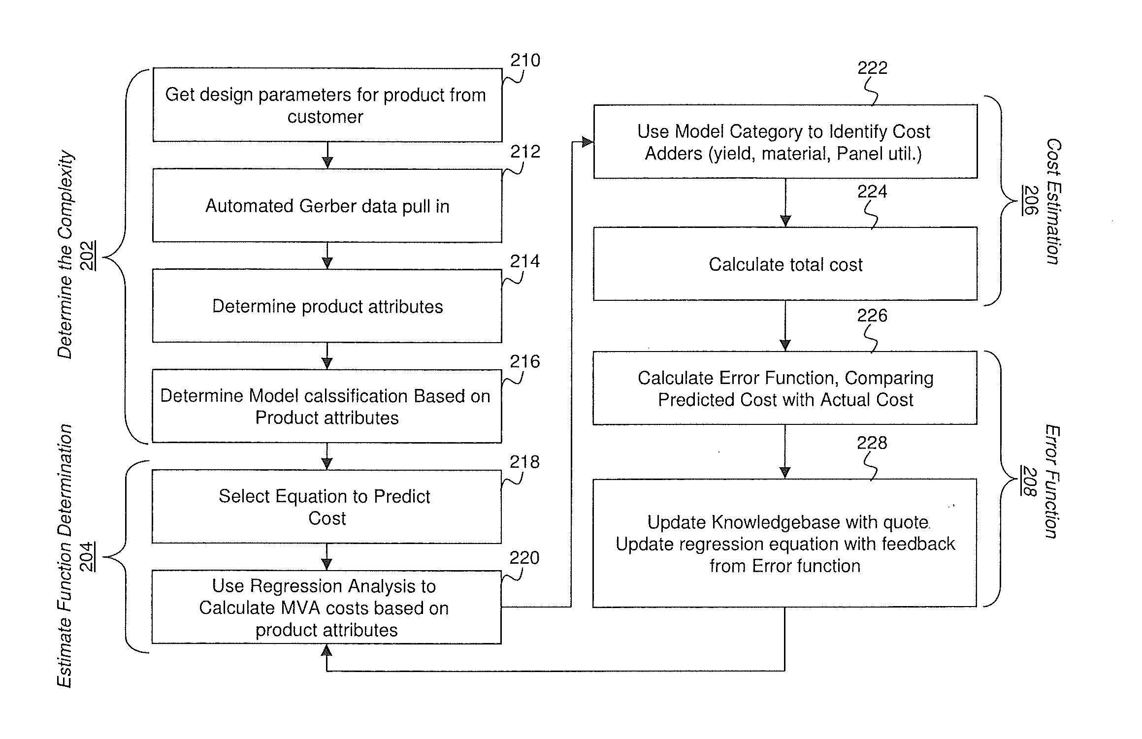
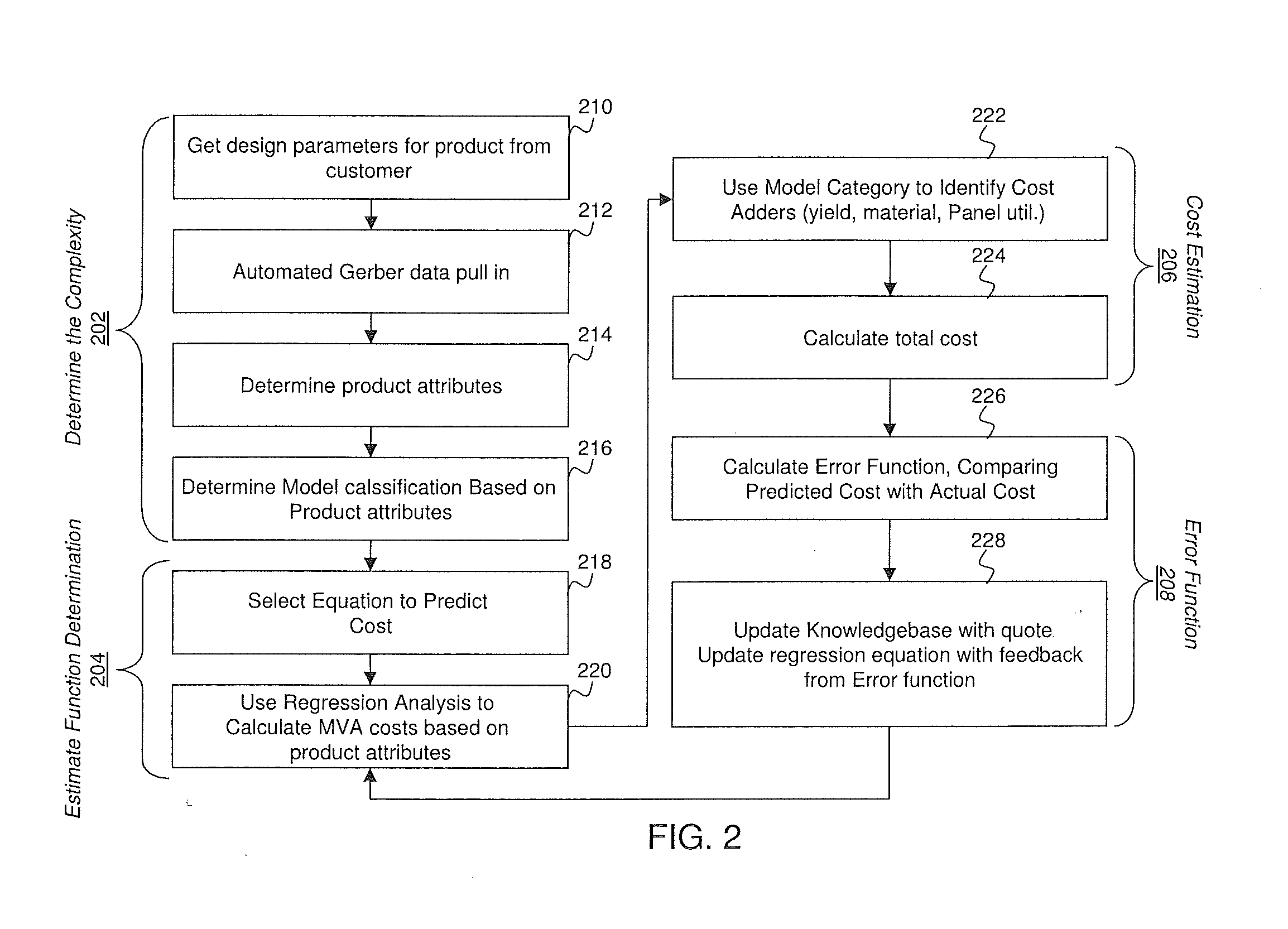
[0014]An embodiment of the present invention provides for advanced modeling of PCB costs. In an embodiment, the design parameters for a PCB are received from a customer in a standard format. Data is extracted from the design parameters, and the product attributes are determined from the data. A product model classification is determined based on the product attributes, and then one of a number of cost prediction equations is selected. The equations are selected to best model the production costs based on the product model classification. Regression analysis is used to calculate a manufacturer's value added costs based n the product attributes. The model classification is used to identify additional costs based on criteria such as anticipated yield, materials of the board, the amount of the panel that is utilized and other factors. A total cost is then calculated based on the regression analysis and the additional costs. Once the manufacturer process is completed, the actual costs ar...


PUM


Abstract

A total cost estimate is calculated based on a set of printed circuit board (PCB) design parameters. The set of PCB design parameters are received, and PCB attributes are extracted from them. Based on the PCB attributes the PCB is classified and a cost equation is calculated. The cost equation is calculated based on a regression analysis of one or more of the PCB attributes. Once the cost equation is calculated, the total cost is computed based on the cost equation.

Description

BACKGROUND[0001]This invention relates generally to processing within a computing environment, and more particularly to advanced methods of modeling printed circuit board production costs.[0002]In the modern electronics and computer industry, there is an ever-increasing demand for printed circuit boards (PCBs) of varying complexity and cost. Organizations often require as many as 400 different electronic PCBs to support even a single server group. The number of components on each card varies between 20 and 900, and the cost per card varies from as low as $5 to as high as $8,000 or more. Annual costs for card assembly for a corporation can run upwards of $1 billion. Therefore, lowering manufacturing costs or improving cycle time for card manufacturing can potentially have a large financial impact.[0003]Estimating the costs of raw cards is an especially challenging task. There are numerous processes that are required to manufacture a raw card, and the cost can be influenced by design ...

Claims


Application Information

Patent Timeline
IPC IPC(8): G06Q10/00
CPCG06F17/5068G06F30/39
Inventor DECUSATIS, CASIMER M.KATOPIS, GEORGE A.KRABBENHOFT, ROGER S.NELSON, TODD A.RAMAKRISHNAN, SREEKANTHRAO, ANURADHATORELLA, JOSEPH H.
Owner IBM CORP
Why Eureka
Try Eureka