

Probe apparatus
a technology of probe apparatus and probe, which is applied in the direction of individual semiconductor device testing, semiconductor/solid-state device testing/measurement, instruments, etc., can solve the problems of diode damage, difficult to accurately measure the current change (di/dt) inherent in the diode, and impaired switching function of the diode, etc., to achieve reliable measurement of static characteristics and dynamic characteristics (the switching characteristics).
- Summary
- Abstract
- Description
- Claims
- Application Information
AI Technical Summary
Benefits of technology
Problems solved by technology
Method used
Image

Examples
first embodiment
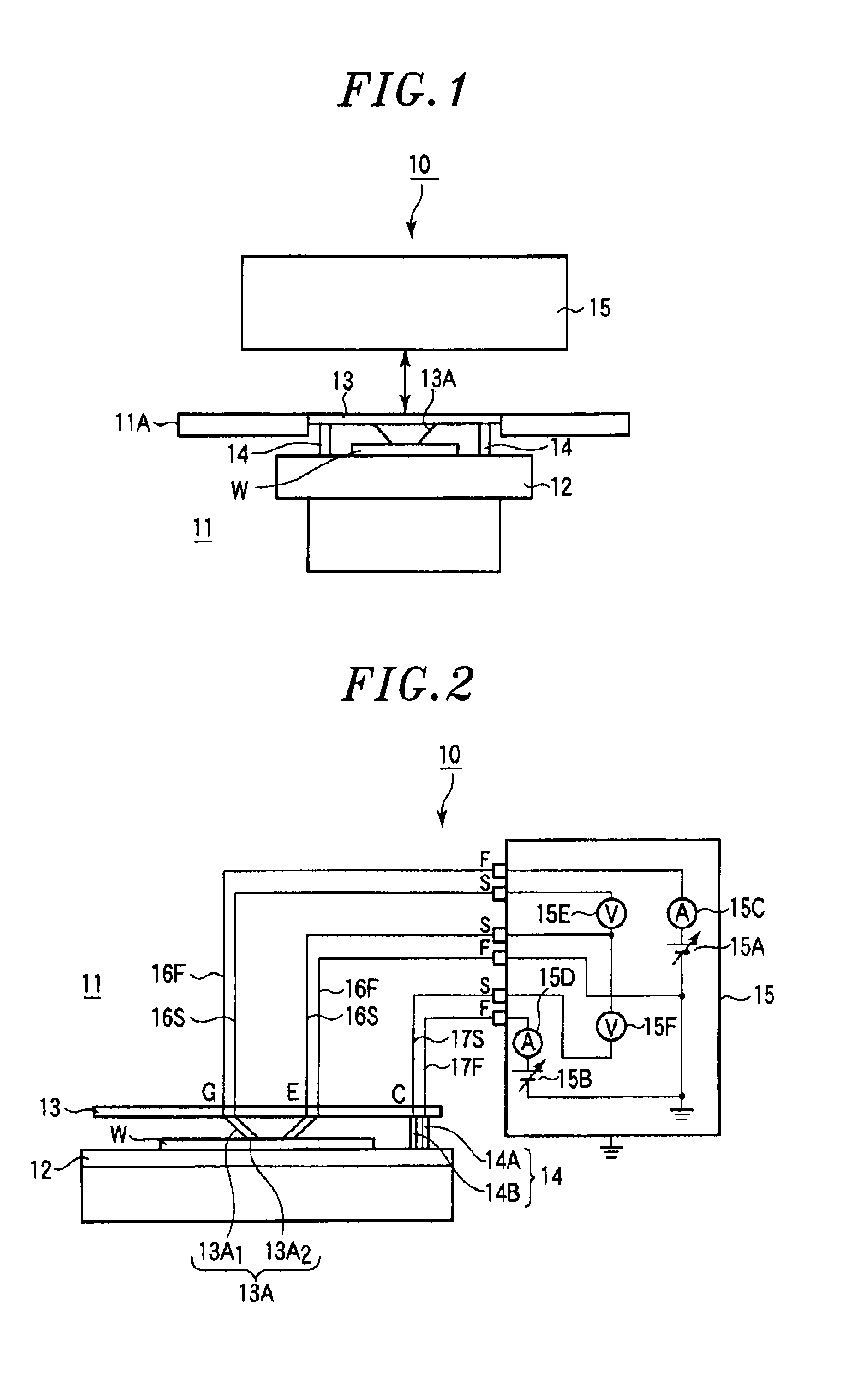
[0040]As shown in FIG. 1, the probe apparatus 10 of the present embodiment is configured to receive, in a prober chamber 11, a semiconductor wafer W transferred from a loader chamber (not shown) for transferring the semiconductor wafer W. Within the prober chamber 11, the probe apparatus 10 measures the current change in a diode included in each of power devices (e.g., IGBTs) formed in the semiconductor wafer W.
[0041]As shown in FIG. 1, a mounting table 12 for holding the semiconductor wafer W is provided in the prober chamber 11 in such a manner as to move in an X-direction, a Y-direction, a Z-direction, and a O-direction. On at least the upper surface of the mounting table 12, a conductive film electrode (not shown) made of electrically conductive metal such as gold or the like is formed as a collector electrode. A vacuum suction means is formed in the mounting table 12 to vacuum-suck the semiconductor wafer W toward the mounting surface of the mounting table 12. A temperature con...
second embodiment
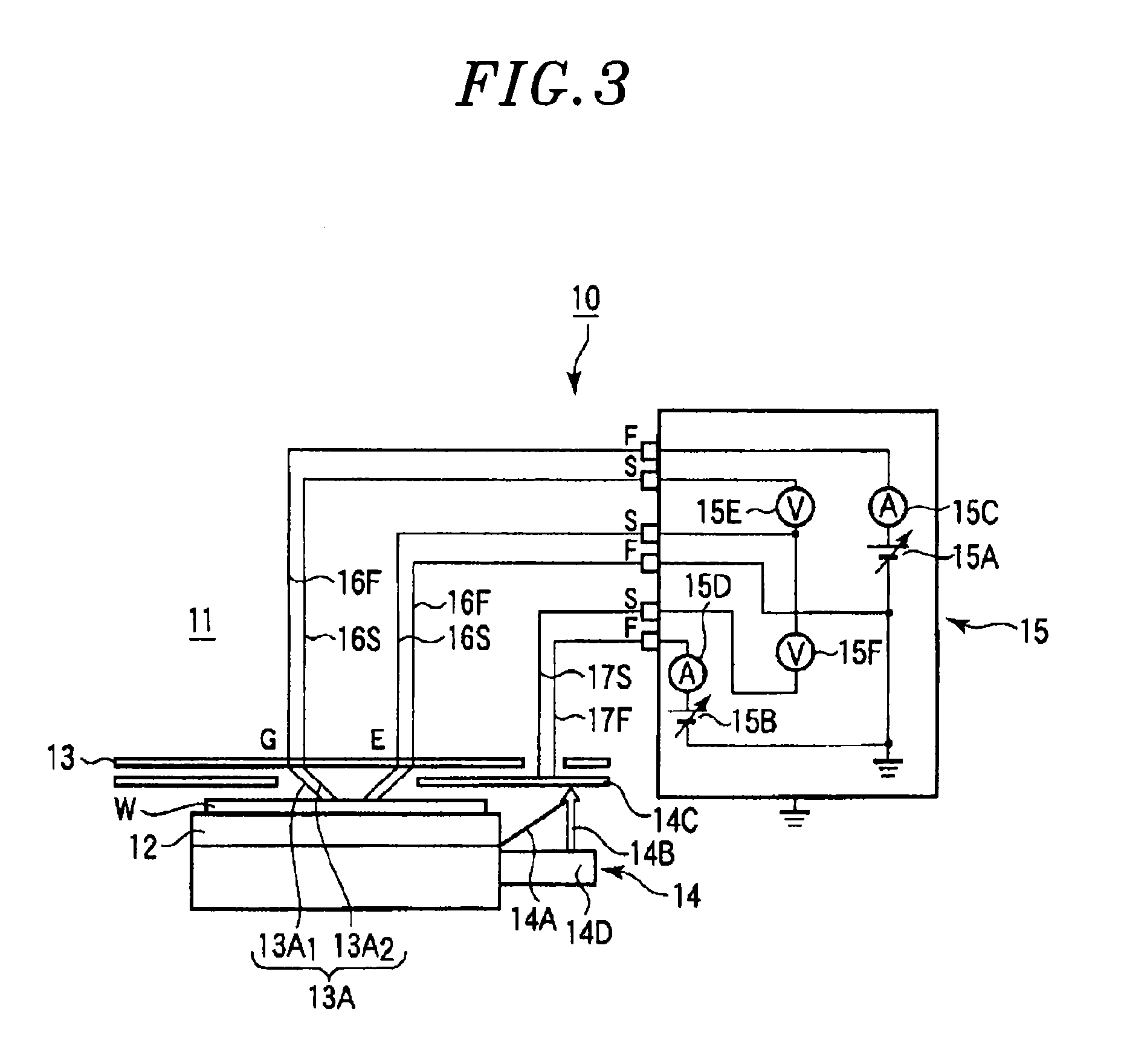
[0057]The probe apparatus of the present embodiment has the same configuration as the configuration of the first embodiment except that a conduction mechanism is provided in place of the conductive pins 14 employed in the first embodiment. The following description will be centered on the features of the probe apparatus of the present embodiment, with the components identical with or similar to those of the probe apparatus 10 of the first embodiment designated by like reference symbols.
[0058]As shown in FIG. 3, the probe apparatus 10 of the present embodiment is configured to receive a semiconductor wafer W provided with a plurality of power devices including diodes in a prober chamber 11 adjacent to a loader chamber (not shown) for transferring the swivel mechanism 12 and to measure the current change of the diode included in each of the power devices under a wafer state. Except the conduction mechanism 14, the probe apparatus 10 of the present embodiment has the same configuration...
third embodiment
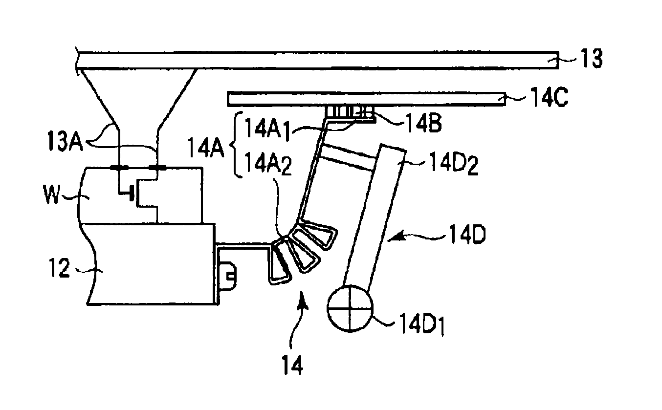
[0066]The conduction mechanism 14 shown in FIG. 4 may be replaced by, e.g., the conduction mechanisms 14 shown in FIGS. 5A through 5D. The conduction mechanisms 14 shown in FIGS. 5A through 5D can promise substantially the same operations and effects as provided by the probe apparatus 10 shown in FIGS. 3 and 4.
[0067]In the conduction mechanism 14 shown in FIG. 5A, the lead conductor 14A shown in FIGS. 4A and 4B is made up of lead wires 14A and the actuator 14D is made up of a cylinder mechanism such as an air cylinder or the like. The actuator 14D includes a cylinder 14D1 using a compressed air as a drive power source and a rod 14D2. Connecting terminals 14B are attached to the tip end of the rod 14D2. As the rod 14D2 is moved up and down, the connecting terminals 14B are electrically connected to or disconnected from a ring conductor 14C. The lead wires 14A are connected to the connecting terminals 14B. The mounting table 12 and the tester 15 are electrically connected to or discon...
PUM
 Abstract
Description
Claims
Application Information