

Liquid crystal display device
- Summary
- Abstract
- Description
- Claims
- Application Information
AI Technical Summary
Benefits of technology
Problems solved by technology
Method used
Image

Examples
first preferred embodiment
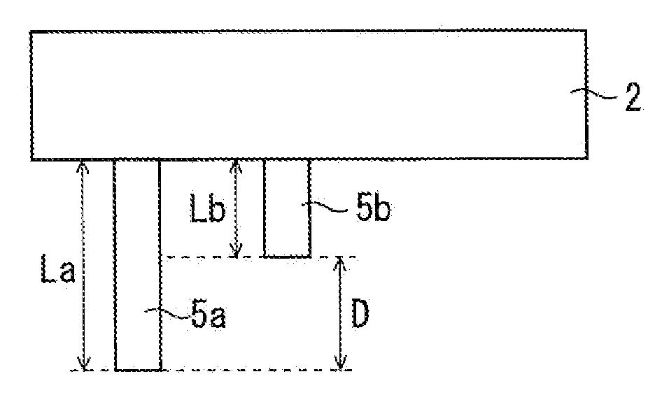
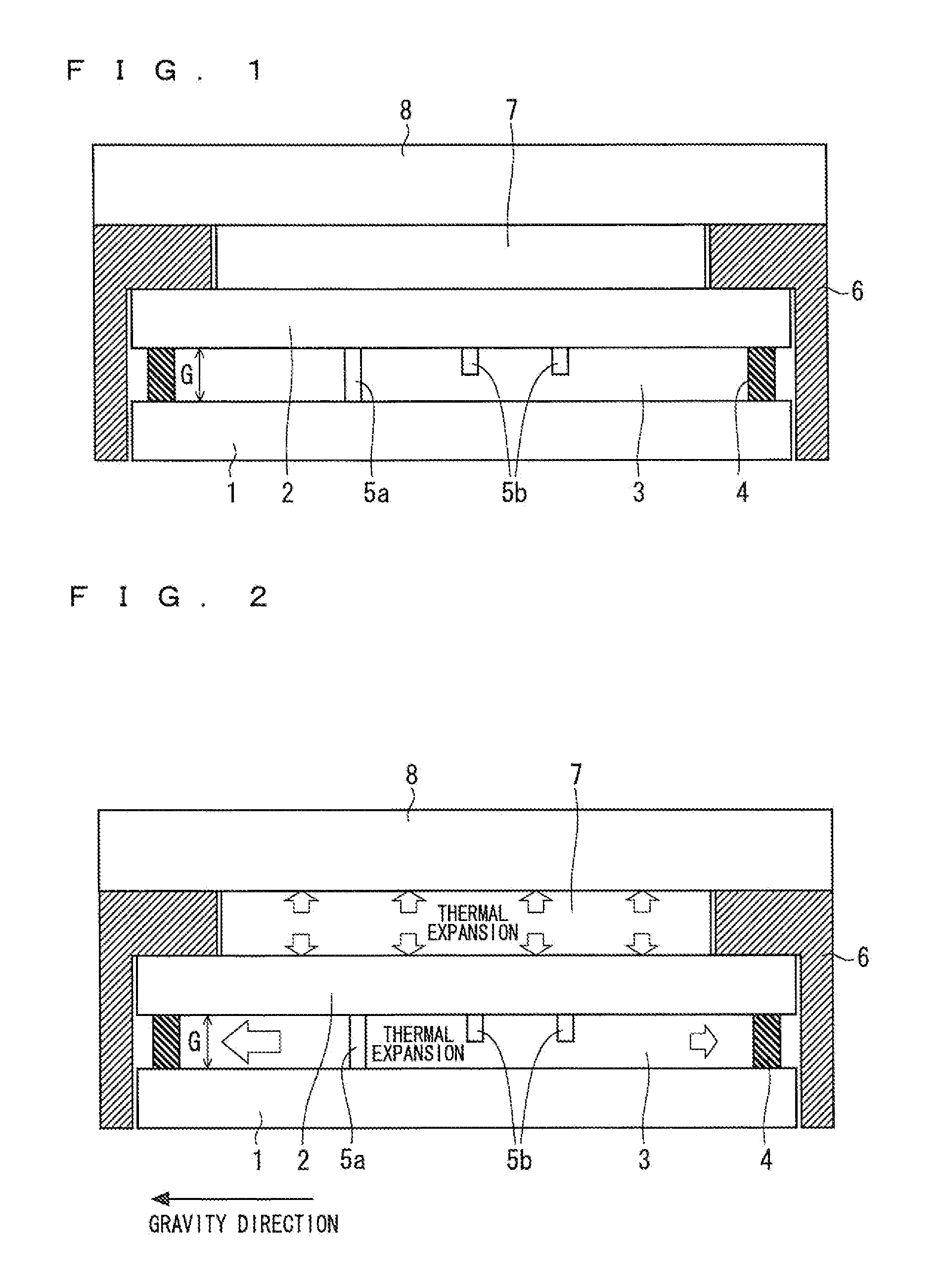
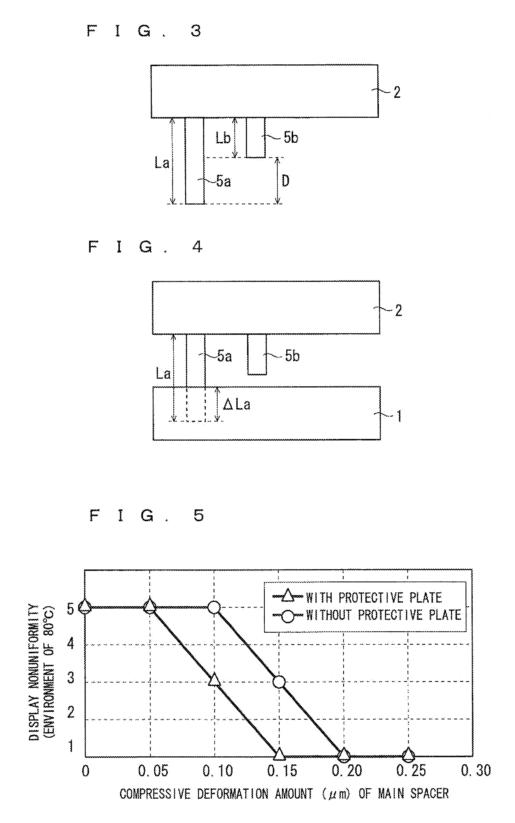
[0027]FIG. 1 is a view showing a configuration of a principle part of a liquid crystal display device according to a first preferred embodiment of the present invention. As in FIG. 1, a display panel (liquid crystal panel) of the liquid crystal display device has a structure in which a liquid crystal 3 is held between a thin-film transistor (TFT) array substrate 1 and a color filter (CF) substrate 2 arranged on a front surface (display surface) side thereof as opposed thereto.
[0028]Although not illustrated, the TFT array substrate 1 is formed by providing, on a transparent substrate such as glass, a pixel electrode of each pixel, a TFT for supplying an image signal to each pixel electrode, a gate wire (scanning signal line) for supplying a drive signal to a gate electrode of each TFT, a source wire (image signal line) for supplying an image signal to a source electrode of the TFT, and the like. Further, the CF substrate 2 is formed by providing, on the rear-side surface (surface opp...
second preferred embodiment
[0049]FIG. 7 is a view showing a configuration of a liquid crystal display device according to a second preferred embodiment. In the present preferred embodiment, the configuration is formed in which the resin layer 7 between the front panel 8 and the liquid crystal panel extends to the above of the peripheral seal 4 of the liquid crystal panel. Other configurations are similar to those of the first preferred embodiment, and descriptions thereof are thus omitted herein.
[0050]In the present preferred embodiment, since the whole of the region filled with the liquid crystal 3 is covered by the resin layer 7, a force of the resin layer 7 to push down the CF substrate 2 at the time of thermal expansion of the resin layer 7 is applied almost uniformly to the whole of the liquid crystal 3. Hence, the liquid crystal 3 is prevented from gathering in the peripheral part of the liquid crystal panel. This can result in prevention of the cell gap G in the peripheral part of the liquid crystal pa...
first modified example
[0052]As described in the first preferred embodiment with reference to FIG. 2, the liquid crystal 3 is likely to flow in the gravity direction, and the cell gap G is likely to increase especially in the lower side part of the liquid crystal panel. For this reason, in the liquid crystal display device according to the second preferred embodiment, it is possible to suppress an increase in the cell gap G in the peripheral part of the liquid crystal panel at least when the resin layer 7 extends to the above of the peripheral seal 4 in the gravity direction.
[0053]Therefore, as shown in FIG. 8, the end of the resin layer 7 on the opposite side to the gravity direction (upper side) may be configured so as not to extend to the above of the peripheral seal 4. In this case, the liquid crystal 3 is more likely to flow to the upper side portion of the liquid crystal panel, but when the cell gap G increases and the compressive deformation amount ΔLa of the main spacers 5a comes close to zero, th...
PUM
 Abstract
Description
Claims
Application Information