High voltage mosfet device

a mosfet device, high-voltage technology, applied in the direction of semiconductor devices, basic electric elements, electrical equipment, etc., can solve the problems of deteriorating voltage-withstanding capability of the overall integrated circuit, and affecting the breakdown voltage of the overall m-type hv mosfet devi

Active Publication Date: 2013-07-25
UNITED MICROELECTRONICS CORP
View PDF3 Cites 3 Cited by
  • Summary
  • Abstract
  • Description
  • Claims
  • Application Information

AI Technical Summary

Problems solved by technology

For simultaneously forming the three types of HV MOSFET devices on the same integrated circuit, the voltage-withstanding capability of the overall integrated circuit is deteriorated because of the limitation of the breakdown voltage of the M-type HV MOSFET device.
Under this circumstance, the voltage-withstanding capability of these specified sites will be impaired, and thus the breakdown voltage of the overall M-type HV MOSFET device is deteriorated.
However, the performance is still unsatisfied.

Method used


Image

  • High voltage mosfet device
  • High voltage mosfet device
  • High voltage mosfet device

Examples


Embodiment Construction

[0022]The present invention will now be described more specifically with reference to the following embodiments. It is to be noted that the following descriptions of preferred embodiments of this invention are presented herein for purpose of illustration and description only. It is not intended to be exhaustive or to be limited to the precise form disclosed.

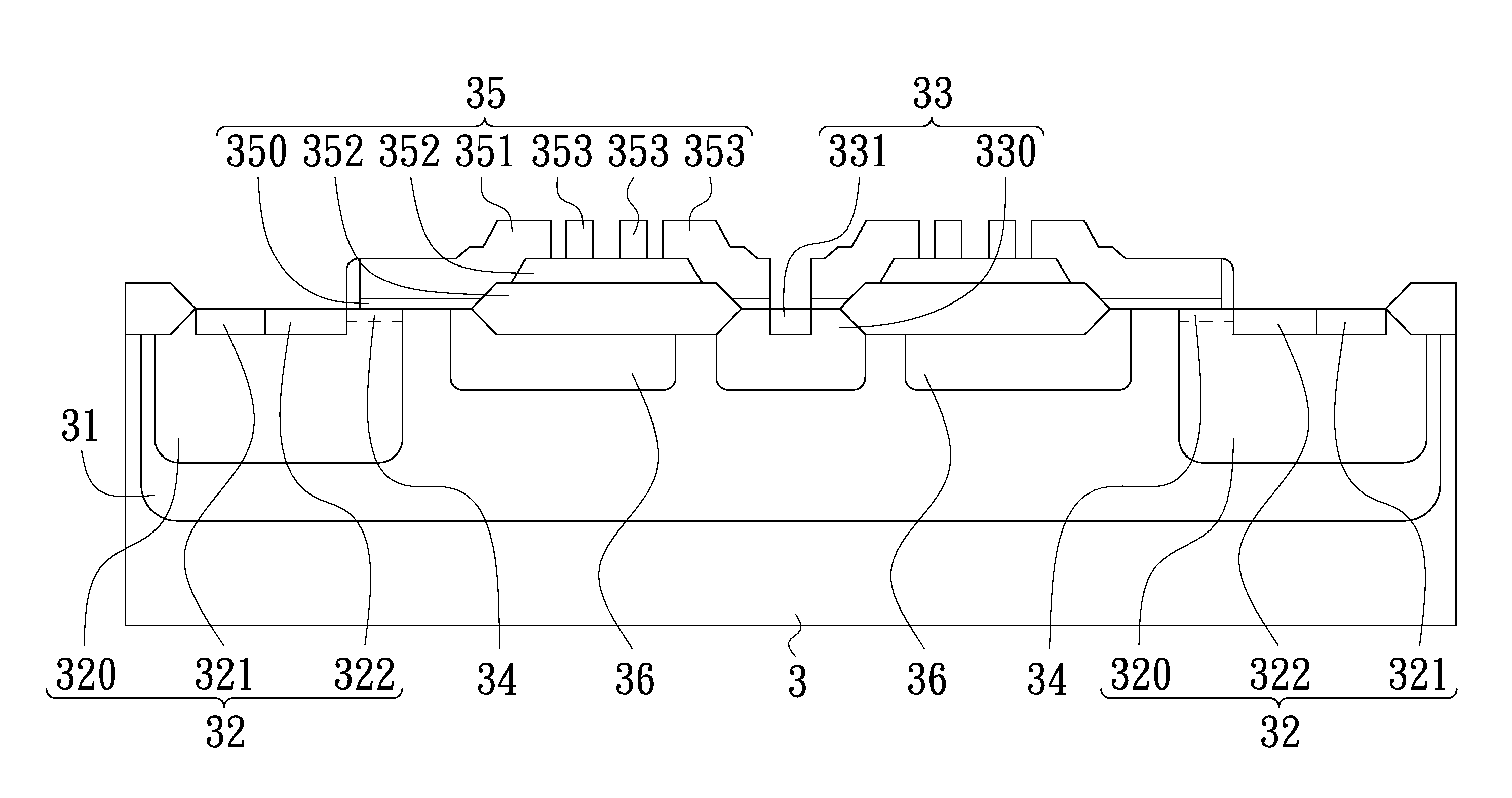
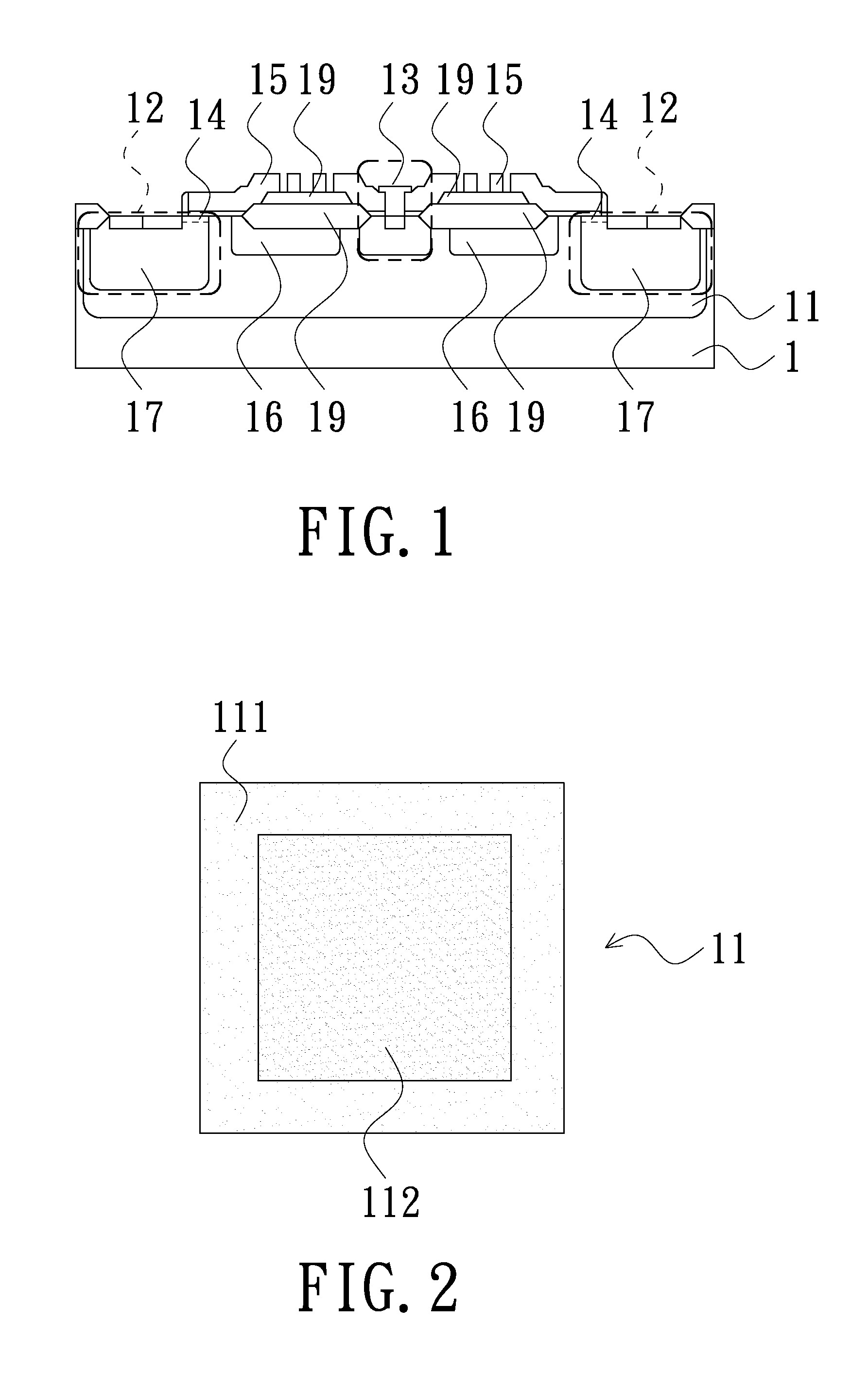
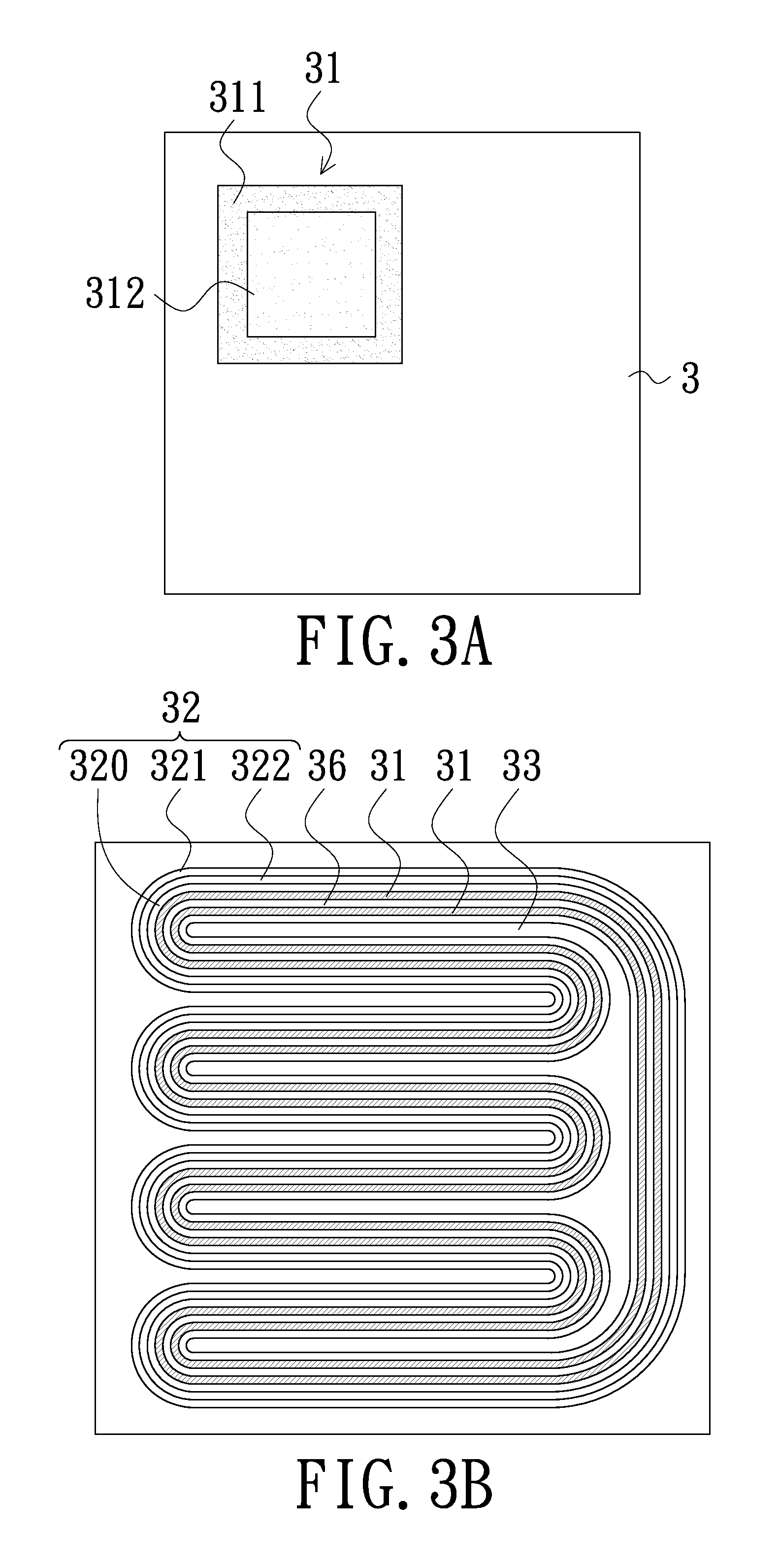
[0023]FIG. 1 is a schematic cross-sectional view illustrating a HV MOSFET device. The HV MOSFET device comprises a substrate 1, a deep well region 11, a source / body region 12, a drain region 13, a gate structure 15, and a first doped region 16. The substrate 1 has a first conductivity type. The deep well region 11 is constructed in the substrate 1. The deep well region 11 has a second conductivity type, wherein the second conductivity type is different from the first conductivity type. The source / body region 12 and the drain region 13 are both formed in the deep well region 11. In addition, a high voltage well region 17 is formed...


PUM


Abstract

A HV MOSFET device includes a substrate, a deep well region, a source / body region, a drain region, a gate structure, and a first doped region. The deep well region includes a boundary site and a middle site. The source / body region is formed in the deep well region and defines a channel region. The first doped region is formed in the deep well region and disposed under the gate structure, and having the first conductivity type. There is a first ratio between a dopant dose of the first doped region and a dopant dose of the boundary site of the deep well region. There is a second ratio between a dopant dose of the first doped region and a dopant dose of the middle site of the deep well region. A percentage difference between the first ratio and the second ratio is smaller than or equal to 5%.

Description

FIELD OF THE INVENTION[0001]The present invention relates to a high voltage MOSFET device, and more particularly to a high voltage MOSFET device with an enhanced breakdown voltage.BACKGROUND OF THE INVENTION[0002]Conventionally, a high voltage metal-oxide-semiconductor field-effect transistor (HV MOSFET) device has a circular configuration. From the top view of the circular HV MOSFET device, the central portion is the drain region, and the outer portion enclosing the drain region is the source region. In addition, the width of the channel region of the circular HV MOSFET device is determined according to the circumference of the intermediate zone between the drain region and the source region. A conventional approach of increasing the conduction current of the HV MOSFET device is to increase the radius of the HV MOSFET device. However, the increase of the radius of the HV MOSFET device will increase the area of the HV MOSFET device.[0003]For increasing the conduction current of the ...

Claims


Application Information

Patent Timeline
Patent Type & Authority Applications(United States)
IPC IPC(8): H01L29/78
CPCH01L21/266H01L29/402H01L29/404H01L29/0878H01L29/7816H01L29/0634H01L29/0696H01L29/66681
Inventor WANG, CHIH-CHUNGLEE, MING-TSUNGHUANG, CHUNG-IHUANG, SHAN-SHILEE, WEN-FANGWU, TE-YUAN
Owner UNITED MICROELECTRONICS CORP
Why Eureka
Try Eureka