High Voltage Semiconductor Power Switching Device

a switching device and high-voltage technology, applied in semiconductor devices, semiconductor/solid-state device details, diodes, etc., can solve the problems of reducing efficiency, not suitable for switching converter applications, and substantial power for driving the bas

Active Publication Date: 2015-04-30
MOSWAY SEMICON
View PDF8 Cites 4 Cited by
  • Summary
  • Abstract
  • Description
  • Claims
  • Application Information

AI Technical Summary

Problems solved by technology

This renders the power for driving the base substantial, especially when the power converter delivers high power to its output.
Therefore, it is not suitable for switching converter application as slow switching transition generates substantial amount of heat at the switching device, as well as degradation of efficiency.
However, due to the actual bipolar base terminal is inside the device, it suffers the same problem of slow switching off as the three terminal Darlington bipolar transistor.

Method used


Image

  • High Voltage Semiconductor Power Switching Device
  • High Voltage Semiconductor Power Switching Device
  • High Voltage Semiconductor Power Switching Device

Examples


Embodiment Construction

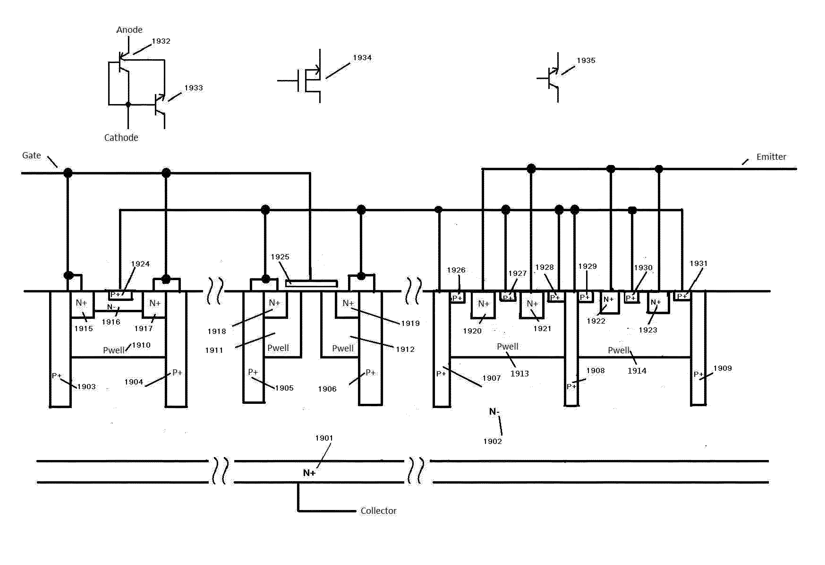
[0151]FIG. 4 is a schematic circuit diagram for an embodiment of the invented three pin high voltage Darlington bipolar power switching device with fast turn off time. High voltage bipolar transistors 401 and 402 form a conventional Darlington bipolar transistor. The current gain of the Darlington transistor is the product of the individual current gain of transistor 401 and transistor 402. Typical current gain of 100 to 400 can be achieved. Therefore, base current to turn on the Darlington transistor is small and the associated power is comparable to the gate drive for power MOSFET power switching device for handling the same output power level. The addition of the diode 403 is to provide a discharging path for the base of transistor 402 during switch off of the Darlington transistor. Hence, diode 403 ensures fast base relaxation and thus fast turn off of this invented power switching device. For diode 403, Schottky diode is more preferred due to the low forward voltage as compared...


PUM


Abstract

A three terminal high voltage Darlington bipolar transistor power switching device includes two high voltage bipolar transistors, with collectors connected together serving as the collector terminal. The base of the first high voltage bipolar transistor serves as the base terminal. The emitter of the first high voltage bipolar transistor connects to the base of the second high voltage bipolar transistor (inner base), and the emitter of the second high voltage bipolar transistor serves as the emitter terminal. A diode has its anode connected to the inner base (emitter of the first high voltage bipolar transistor, or base of the second high voltage bipolar transistor), and its cathode connected to the base terminal. Similarly, a three terminal hybrid MOSFET / bipolar high voltage switching device can be formed by replacing the first high voltage bipolar transistor of the previous switching device by a high voltage MOSFET.

Description

BACKGROUND OF THE INVENTION[0001]The present invention relates to high voltage semiconductor switching devices. The invention more particularly, although not exclusively, relates to switching device for switching converter applications.[0002]Prior art switching converter circuits are shown in FIGS. 1 and 2. FIG. 1 shows an isolated constant voltage output switching converter while FIG. 2 shows a non-isolated switching converter having constant current output for driving LED lighting.[0003]In both FIGS. 1 and 2, the selection of the power switching device (115 and 215 respectively) is a key decision. Bipolar transistor and MOSFET are typical candidates for power switching device. Bipolar transistors are much less costly than the MOSFET at the same power rating. However, MOSFETs are normally more preferred, especially at high power levels, due to the following reasons:[0004]a. Bipolar transistors require continuous base current to keep them in the turn on state while MOSFETs only requ...

Claims


Application Information

Patent Timeline
Patent Type & Authority Applications(United States)
IPC IPC(8): H01L27/06H01L21/56H01L29/739H01L29/872
CPCH01L27/0647H01L29/872H01L29/7396H01L27/0635H01L21/561H01L2224/48137H01L2224/49171H01L2224/48247H01L2924/13055H01L2924/13091H01L2924/00H01L21/565H01L21/8249H01L21/84H01L23/535H01L27/0825H01L27/1203H01L29/0634H01L29/0804H01L29/0821H01L29/0847H01L29/1004H01L29/1095H01L29/41708H01L29/41758H01L29/42304H01L29/42356H01L29/42364H01L29/45H01L29/4916
Inventor TSE, CHIU-SING CELEMENTCHAN, ON-BON PETERTANG, CHI-KEUNG
Owner MOSWAY SEMICON
Why Eureka
Try Eureka