Method for integrated manufacturing of split gate flash memory with high voltage MOSFETS

a manufacturing method and high-voltage technology, applied in the direction of basic electric elements, electrical equipment, semiconductor devices, etc., can solve the problems of increasing the cycle time to reduce the wafer throughput, adverse effects, and adding to production costs

Inactive Publication Date: 2006-02-14
TAIWAN SEMICON MFG CO LTD
View PDF4 Cites 4 Cited by
  • Summary
  • Abstract
  • Description
  • Claims
  • Application Information

AI Technical Summary

Problems solved by technology

The incompatible processes require different and separate processing steps which add to the cost of production including increased cycle time to decrease wafer throughput.
In addition, the thermal cycles required by separate process may have an adverse effect on different types of transistors, for example by undesirably subjecting one transistor type in the embedded or integrated device to thermal cycling processes which have an adverse effect on, for example, dopant profiles, thereby altering electrical properties.

Method used


Image

  • Method for integrated manufacturing of split gate flash memory with high voltage MOSFETS
  • Method for integrated manufacturing of split gate flash memory with high voltage MOSFETS
  • Method for integrated manufacturing of split gate flash memory with high voltage MOSFETS

Examples


Embodiment Construction

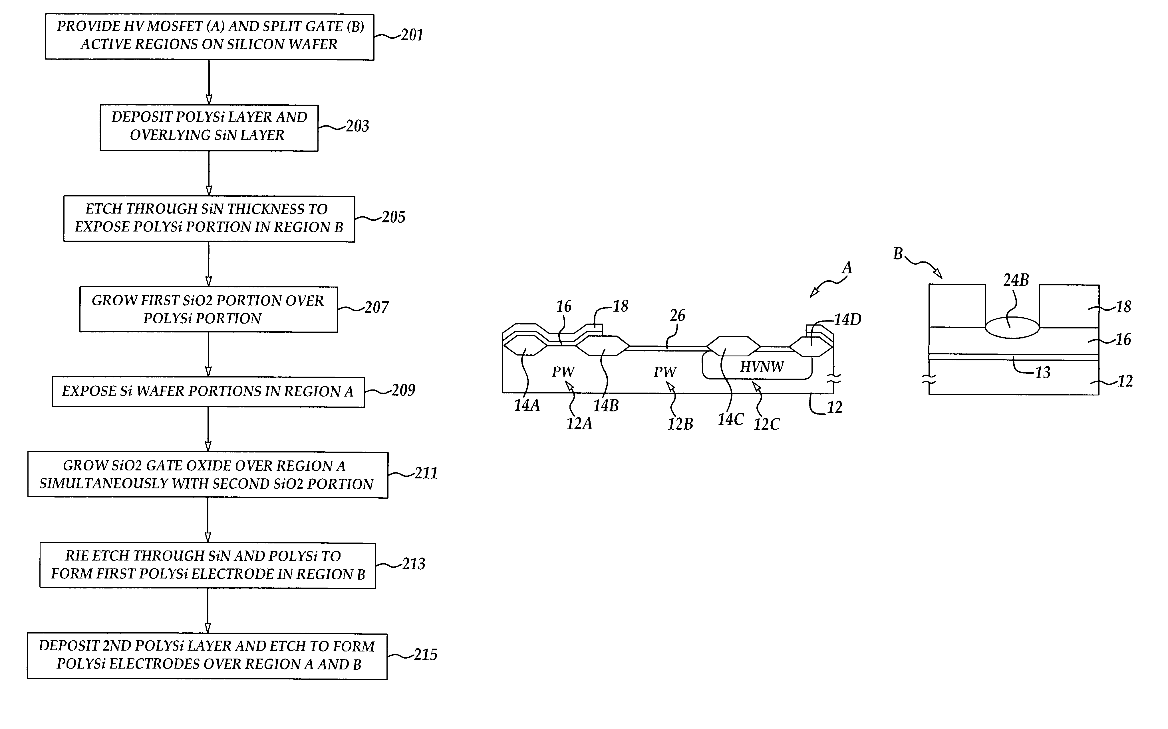
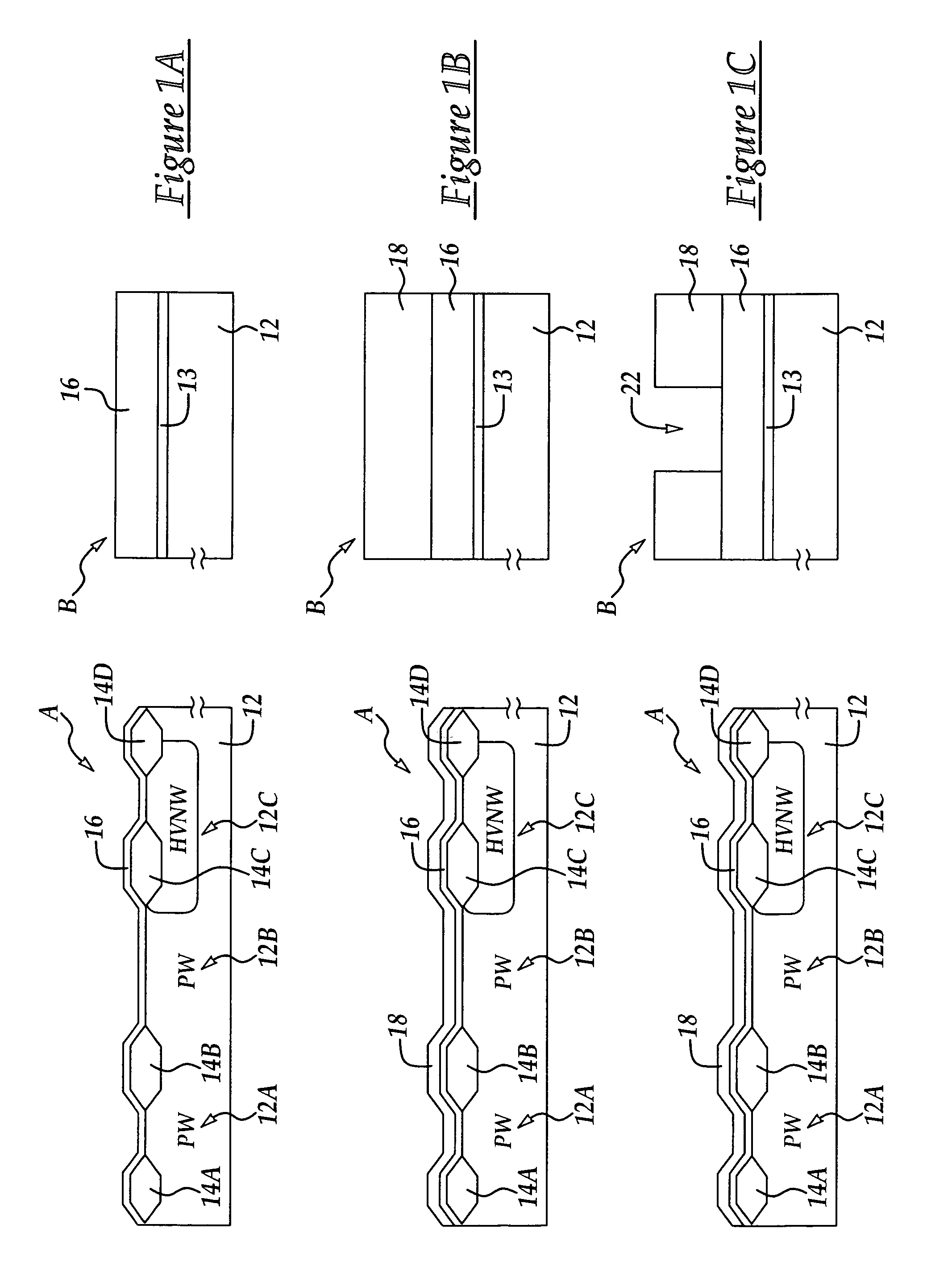
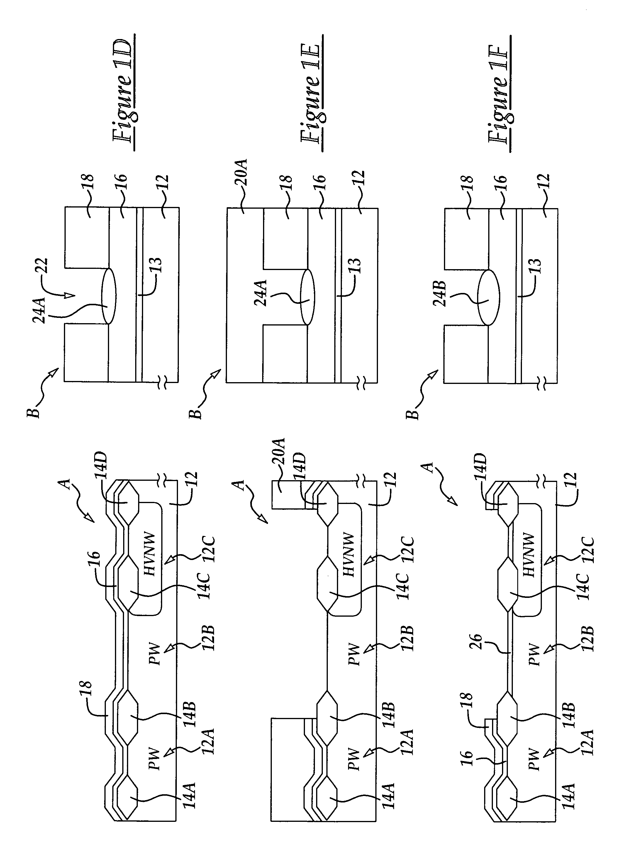
[0011]Referring to FIG. 1A is are shown juxtaposed cross sectional representations of portions of a process wafer. For example, wafer portion A, representing a portion of a high Voltage (HV) device region is shown juxtaposed to wafer portion B, representing a portion of a flash memory cell including a portion of a split gate MOSFET whereby wafer portions A and B are shown at parallel stages in an integrated manufacturing process. It will be appreciated that wafer portions A and B of the process wafer represent parallel stages in manufacture showing the parallel effects of processing steps of the exemplary embodiment of the present invention.

[0012]Shown in FIG. 1A, portion A, are field oxide (FOX) LOCOS isolation structures 14A, 14B, 14C, and 14D formed overlying silicon substrate 12 including doped P-Well regions 12A and 12B, and HV N-well doped region 12C. The FOX LOCOS isolation structures are formed following formation of the doped regions, for example by first patterning an over...


PUM


Abstract

A method for integrated processing of a high Voltage MOSFET device and a split gate MOSFET device whereby a novel method is provided to form the split gate device and the high voltage MOSFET device in parallel processing steps including an oxide formation step whereby an oxide spacer layer in a split gate device is formed using about the same overall thermal budget while forming in parallel a thick gate oxide for a an embedded high voltage MOSFET device.

Description

FIELD OF THE INVENTION[0001]This invention generally relates to microelectronic integrated circuit (IC) semiconductor device fabrication and more particularly to a method for integrated manufacturing of split gate flash memory with high voltage MOSFETS.BACKGROUND OF THE INVENTION[0002]With increasing demands for embedded memory type structures, mixed-signal circuits, and system on chip (SOC) IC design, it has become necessary to form multiple transistor structures on a single die to achieve integrated functioning of the different transistor structures. For example, transistors with different structures and functions typically operate under different current and voltage parameters requiring different processing steps for the various transistors. For example, in the formation of high Voltage MOSFETS, for example operating at Voltages higher than about 30 Volts, for example, about 40 to about 60 Volts, the gate oxide is required to be much thicker for proper operation and to avoid diel...

Claims


Application Information

Patent Timeline
Patent Type & Authority Patents(United States)
IPC IPC(8): H01L21/8238H01L21/8247H01L27/105H01L27/115
CPCH01L27/105H01L27/11536H01L27/11526H01L27/115H10B41/40H10B41/44H10B69/00
Inventor WU, HAW-CHUANTZENG, JIANN-TYNGHO, DAVID
Owner TAIWAN SEMICON MFG CO LTD
Why Eureka
Try Eureka