Touch-sensing module
- Summary
- Abstract
- Description
- Claims
- Application Information
AI Technical Summary
Benefits of technology
Problems solved by technology
Method used
Image
Examples
Embodiment Construction
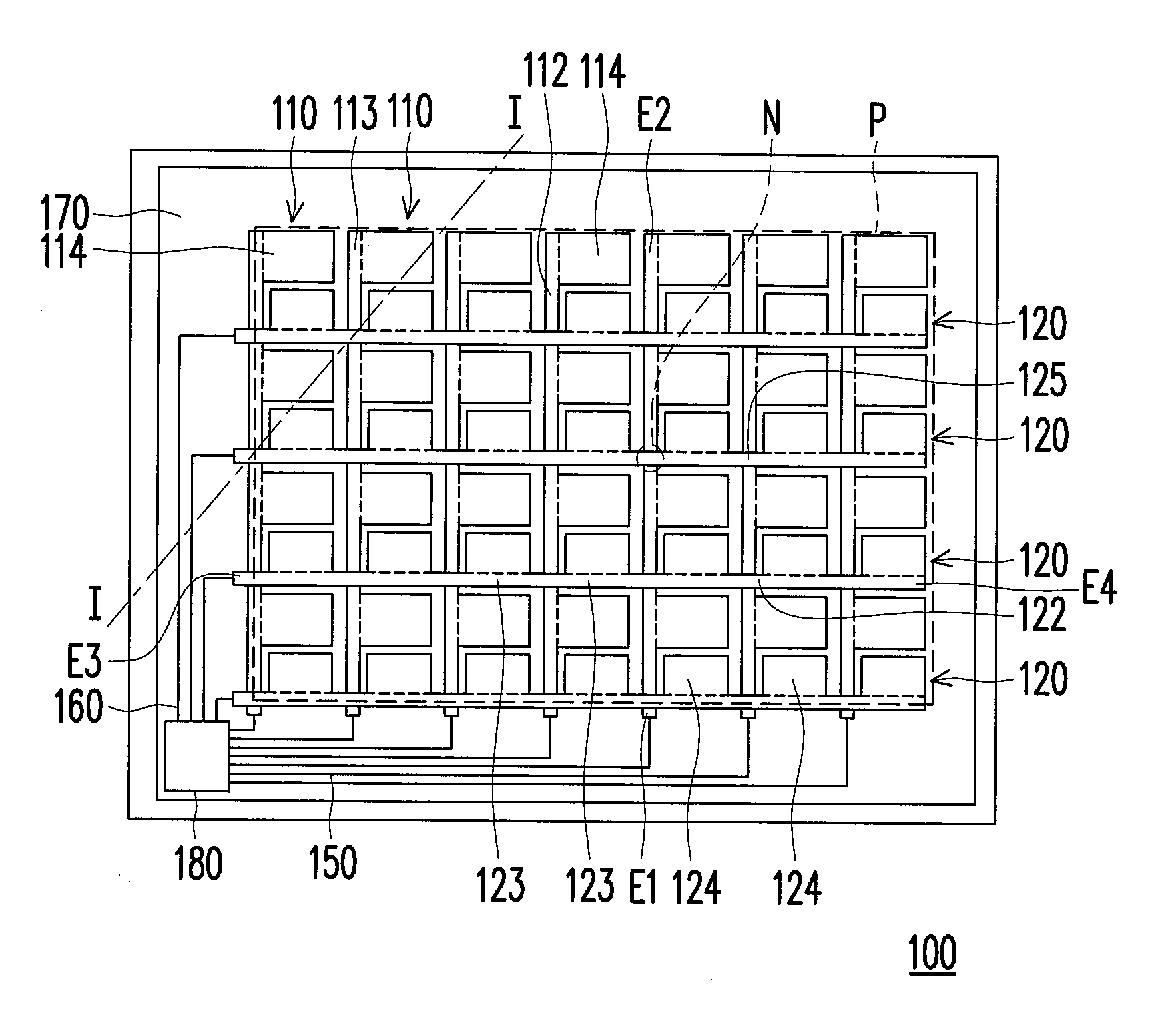
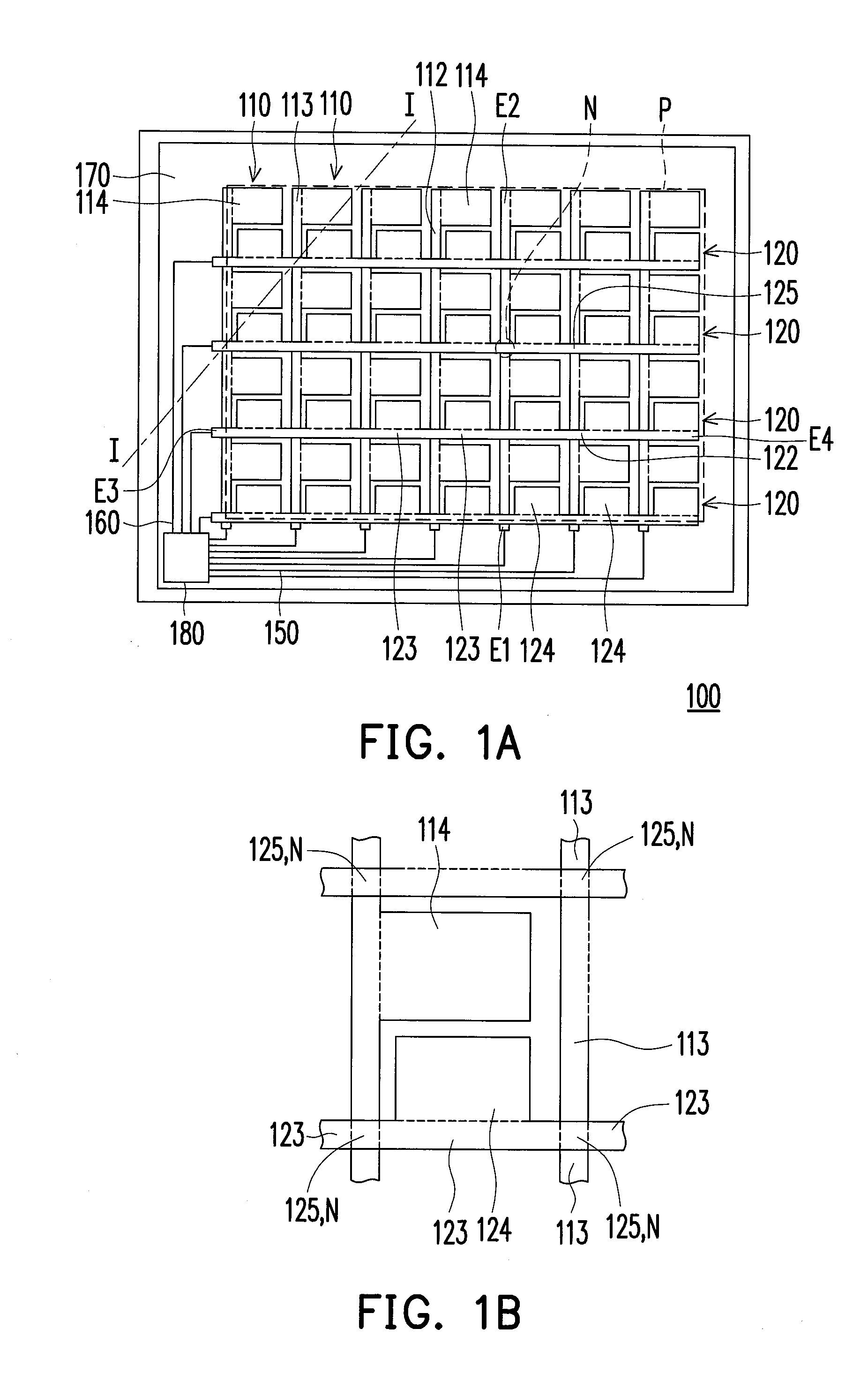
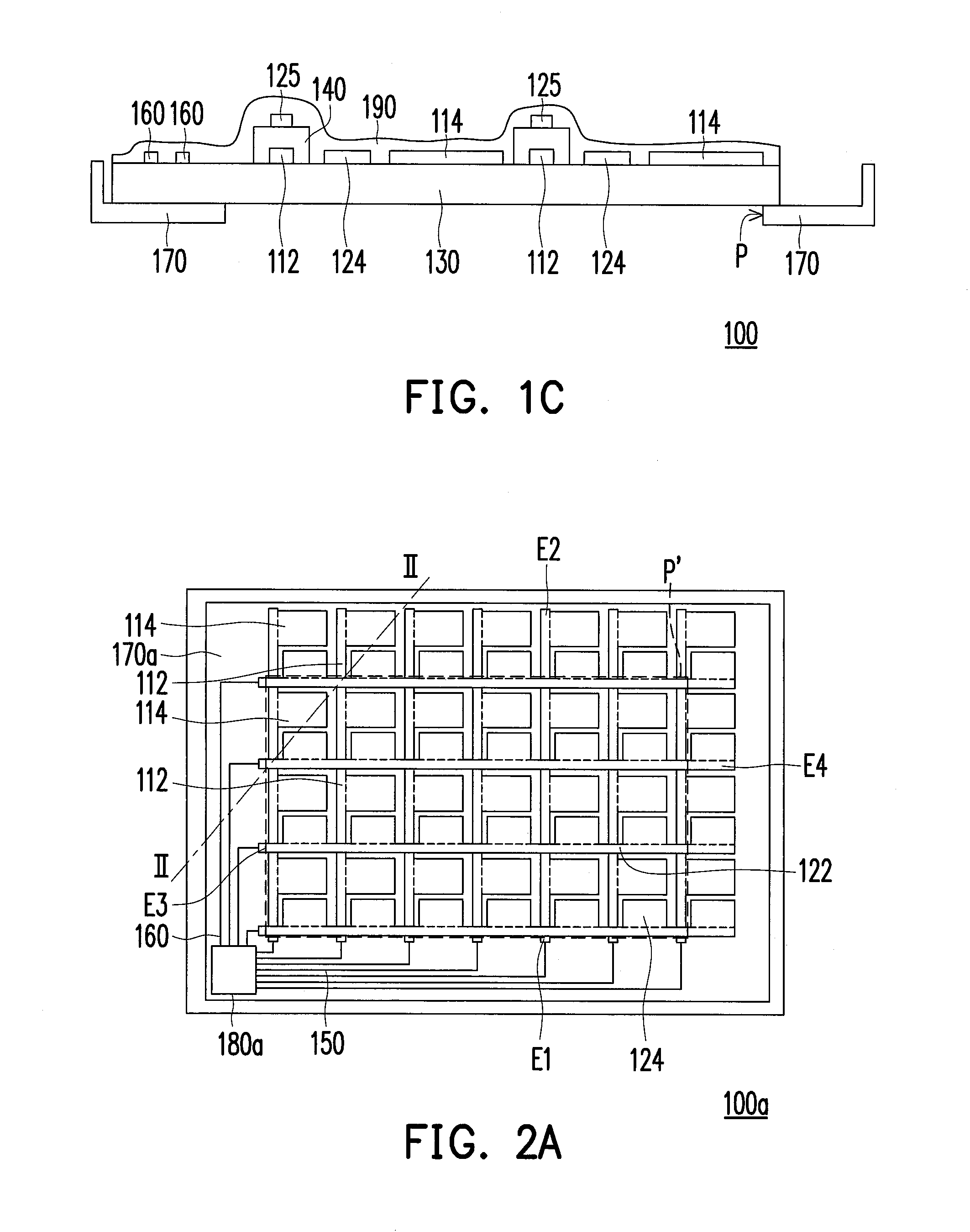
[0019]FIG. 1A is a schematic rear view illustrating a touch-sensing module according to an embodiment of the invention. FIG. 1B is an enlarged partial view illustrating the touch-sensing module 100 illustrated in FIG. 1A. FIG. 1C is a schematic cross-sectional view illustrating a touch-sensing module illustrated in FIG. 1A along line I-I. To simplify the illustration of drawings, FIG. 1C illustrates a substrate which is omitted and not shown in FIG. 1A. Referring to FIG. 1A and FIG. 1C, the touch-sensing module 100 of the present embodiment includes a plurality of first sensing strings 110 and a plurality of second sensing strings 120. Each of the first sensing strings 110 includes a first strip-shaped conductive line 112 and a plurality of first sensing pads 114. The first sensing pads 114 are connected to a same side of the first strip-shaped conductive line 112. For example, the first sensing pads 114 of each of the first sensing strings 110 are all located at the right side of t...
PUM
| Property | Measurement | Unit |
|---|---|---|
| Time | aaaaa | aaaaa |
| Electrical conductor | aaaaa | aaaaa |
| Transparency | aaaaa | aaaaa |
Abstract
Description
Claims
Application Information


