Organic light emitting display device and method of manufacturing the same

a technology of light-emitting display and organic material, which is applied in the direction of thermoelectric device junction materials, semiconductor devices, electrical apparatus, etc., can solve the problems of easy cracking of the bottom layer of the sub-pixel and the easy cracking of the bottom layer of the partition wall, and achieve the effect of stable organic light-emitting display and reducing the risk of dark spots

Active Publication Date: 2013-12-05
SAMSUNG DISPLAY CO LTD
View PDF1 Cites 6 Cited by
  • Summary
  • Abstract
  • Description
  • Claims
  • Application Information

AI Technical Summary

Benefits of technology

[0008]In order to realize a more stable organic light emitting display device, embodiments of the present invention are directed to a structure capable of reducing the risk of dark spots occurring.

Problems solved by technology

The sub pixels are separated from each other into individual regions by partition walls, such as pixel defining layers or spacers, and bottom layers of the sub pixels may easily crack due to the partition walls when an external force is applied.
In other words, since a partition wall, such as a pixel defining layer or spacer, protrudes upward between the sub pixels to form a stepped portion, when an external force is applied to the partition wall, stress is concentrated in the stepped portion, and thus the bottom layer of the partition wall is easily cracked.

Method used


Image

  • Organic light emitting display device and method of manufacturing the same
  • Organic light emitting display device and method of manufacturing the same
  • Organic light emitting display device and method of manufacturing the same

Examples


Embodiment Construction

[0028]Hereinafter, exemplary embodiments of the present invention will be described in detail with reference to the accompanying drawings.

[0029]In drawings, like reference numerals denote like elements. While describing embodiments of the present invention, detailed descriptions about related well-known functions or configurations that may diminish the clarity of the points of the present invention are omitted.

[0030]In the drawings illustrating embodiments of the present invention, some layers or regions may be exaggerated for clarity. Also, it will be understood that when a portion, such as a layer, film, region, or plate, is referred to as being “on” another portion, it can be “directly on” or an intervening portion may be present.

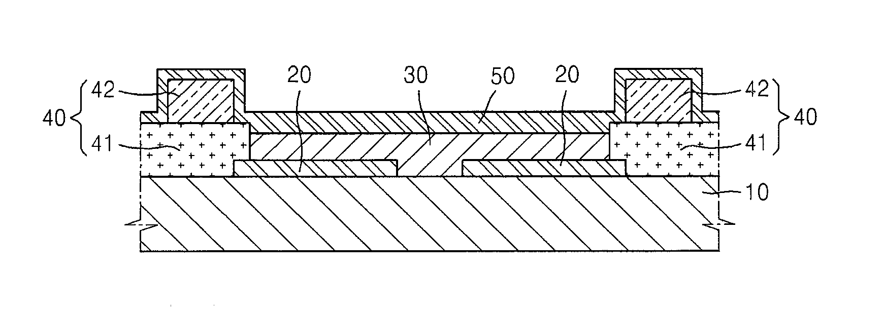
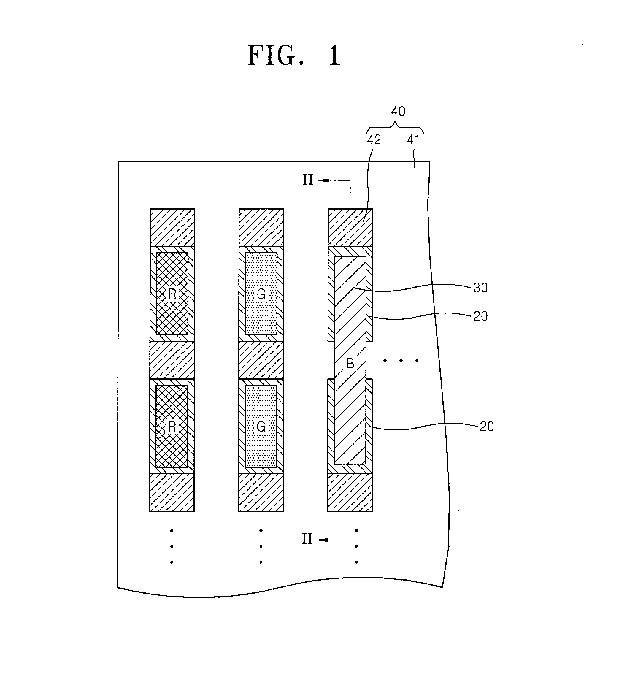
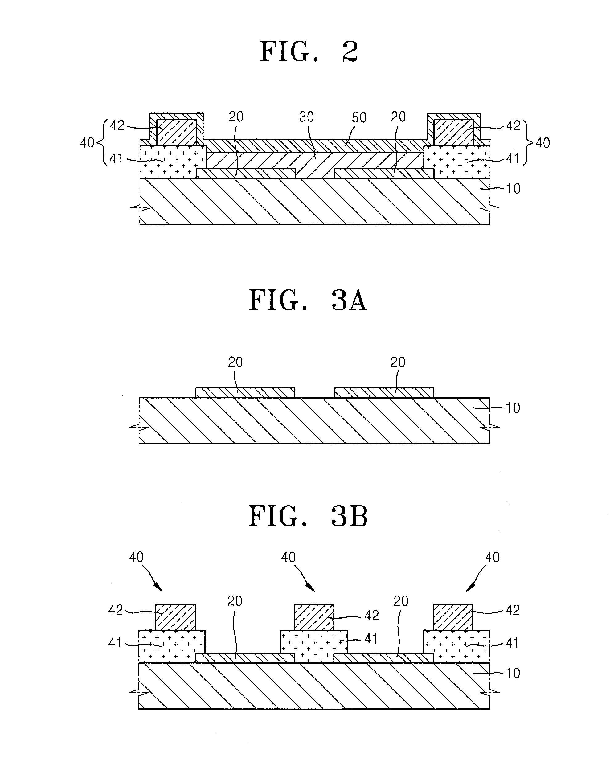
[0031]FIG. 1 is a plan view of sub pixels of an organic light emitting display device according to an embodiment of the present invention, and FIG. 2 is a cross-sectional view taken along a line II-II of FIG. 1.

[0032]Referring to FIG. 1, the organic ligh...


PUM


Abstract

An organic light emitting display device including a plurality of sub pixels, each of the sub pixels including an emissive layer between a pixel electrode and a counter electrode; and a partition wall defining regions of the plurality of sub pixels, wherein the partition wall is not located between at least one pair of adjacent sub pixels of the plurality of sub pixels.

Description

CROSS-REFERENCE TO RELATED PATENT APPLICATION[0001]This application claims priority to and the benefit of Korean Patent Application No. 10-2012-0057473, filed on May 30, 2012, in the Korean Intellectual Property Office, the disclosure of which is incorporated herein in its entirety by reference.BACKGROUND[0002]1. Field[0003]Embodiments of the present invention relate to an organic light emitting display device, and more particularly, to an organic light emitting display device having a spacer structure so as to reduce the occurrence of dark spots caused by short circuits, and a method of manufacturing the same.[0004]2. Description of the Related Art[0005]Generally, an organic light emitting display device realizes (or produces) a color by emitting light when recombining holes and electrons respectively injected from an anode and a cathode in a light emitting unit, and has a stacked structure wherein the light emitting unit is located between a pixel electrode that acts as the anode ...

Claims


Application Information

Patent Timeline
Patent Type & Authority Applications(United States)
IPC IPC(8): H01L27/32H01L51/56
CPCH10K59/353H10K59/173H10K59/122H10K2102/341H01L29/6656H10K59/35
Inventor HONG, SANG-MIN
Owner SAMSUNG DISPLAY CO LTD
Why Eureka
Try Eureka