Distributed element filters for ultra-broadband communications

a distributed element and ultra-broadband technology, applied in waveguides, coatings, electrical equipment, etc., can solve the problems of low power handling capability, large insertion loss, and large size of ceramic thin-film based filters for high frequencies,

Inactive Publication Date: 2014-02-27
HARRIS CORP
View PDF2 Cites 12 Cited by
  • Summary
  • Abstract
  • Description
  • Claims
  • Application Information

AI Technical Summary

Benefits of technology

[0006]Embodiments of the invention concern a method for constructing a radio frequency filter. The method includes steps involving depositing on a surface of a dielectric substrate a plurality of layers including at least one layer each of a conductive material, a dielectric material, and a sacrificial material. A deposition of the at least one layer of conductive material is controlled to form at least one transmission line including a shield and a center conductor disposed coaxially within the shield. The deposition of the conductive material is further controlled to form at least one distributed filter element electrically coupled to the center conductor, and at least one housing electrically coupled to the shield. The housing includes walls enclosing at least one distributed filter element. The method also includes dissolving at least one layer of the sacrificial material to form a channel disposed within at least one shield. The channel thus created results in the formation of a first clearance space between the center conductor and each of one or more shield walls, such that the center conductor resides in the channel spaced apart from the shield walls. The dissolving of the sacrificial material also results in the formation of a interior space disposed within at least one housing. The interior space includes a second gap or clearance space between at least one distributed filter element and each of the housing walls, such that at least one distributed filter element resides within the interior space, and is separated from the housing walls by a gap.
[0007]The invention also includes a radio frequency filter assembly. The filter assembly includes a dielectric substrate and a plurality of layers of a material arranged in a stack. The layers include a plurality of conductive material layers which are arranged to form at least one transmission line including a shield and a center conductor disposed coaxially within the shield. The conductive material layers also form at least one distributed filter element electrically coupled to the center conductor, and at least one housing electrically coupled to the shield. The housing is comprised of walls which enclose at least one distributed filter element. At least one layer of the dielectric material is arranged to form a first set of two or more tabs extending from at least one the shield wall to the center conductor at spaced intervals along an elongated length of the center conductor. One or more layers of the sacrificial material fills a channel defined by at least one shield, and a first clearance space between the center conductor and each of one or more shield walls. The sacrificial material also fills an interior space defined by at least one housing, including a second clearance space between at least one distributed filter element and each of the plurality of housing walls, such that at least one distributed filter element resides in the interior space separated from the housing walls by a gap. The sacrificial material is configured to support the center conductor and the distributed filter element during a manufacturing process which includes the formation of the tabs. The sacrificial material is one which is selectively dissolvable after the manufacturing process is complete without causing damaging or degrading the structures formed by the conductive material and the dielectric material.

Problems solved by technology

However, existing filters for high frequencies (e.g. 10 GHz to 300 GHz) are known to suffer from certain limitations.
Conversely, ceramic thin-film based filters can be relatively small in size but have low power handling capability.
A further drawback of thin film ceramic filters operable at these frequency ranges is that they typically have a relatively large insertion loss.
These processes provide an alternative to traditional thin film technology, but also present new design challenges pertaining to their effective utilization for advantageous implementation of various RF devices.

Method used


Image

  • Distributed element filters for ultra-broadband communications
  • Distributed element filters for ultra-broadband communications
  • Distributed element filters for ultra-broadband communications

Examples


Embodiment Construction

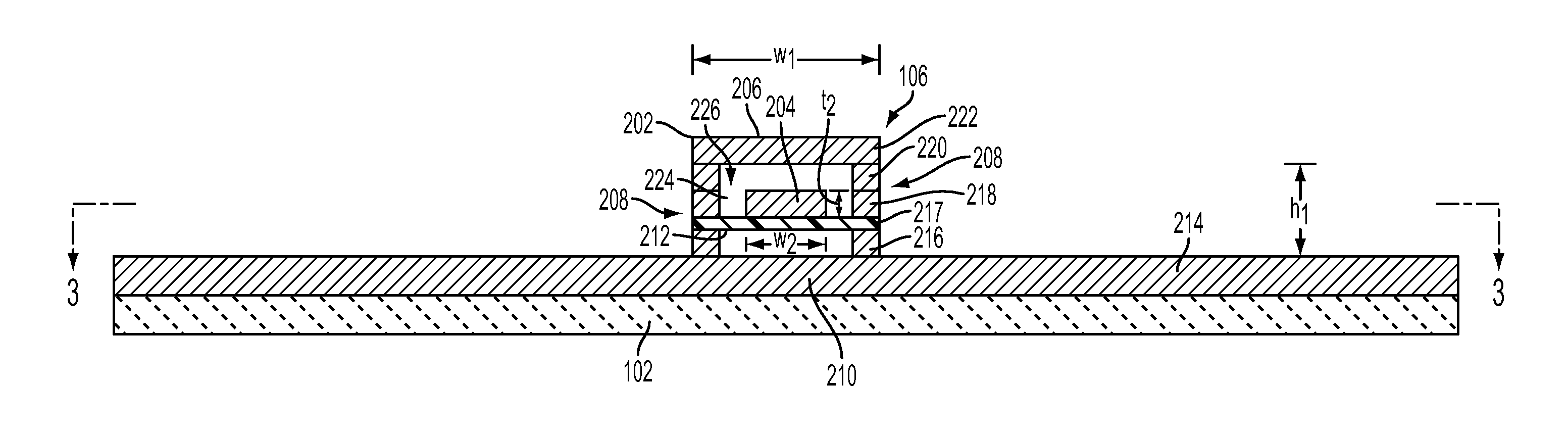
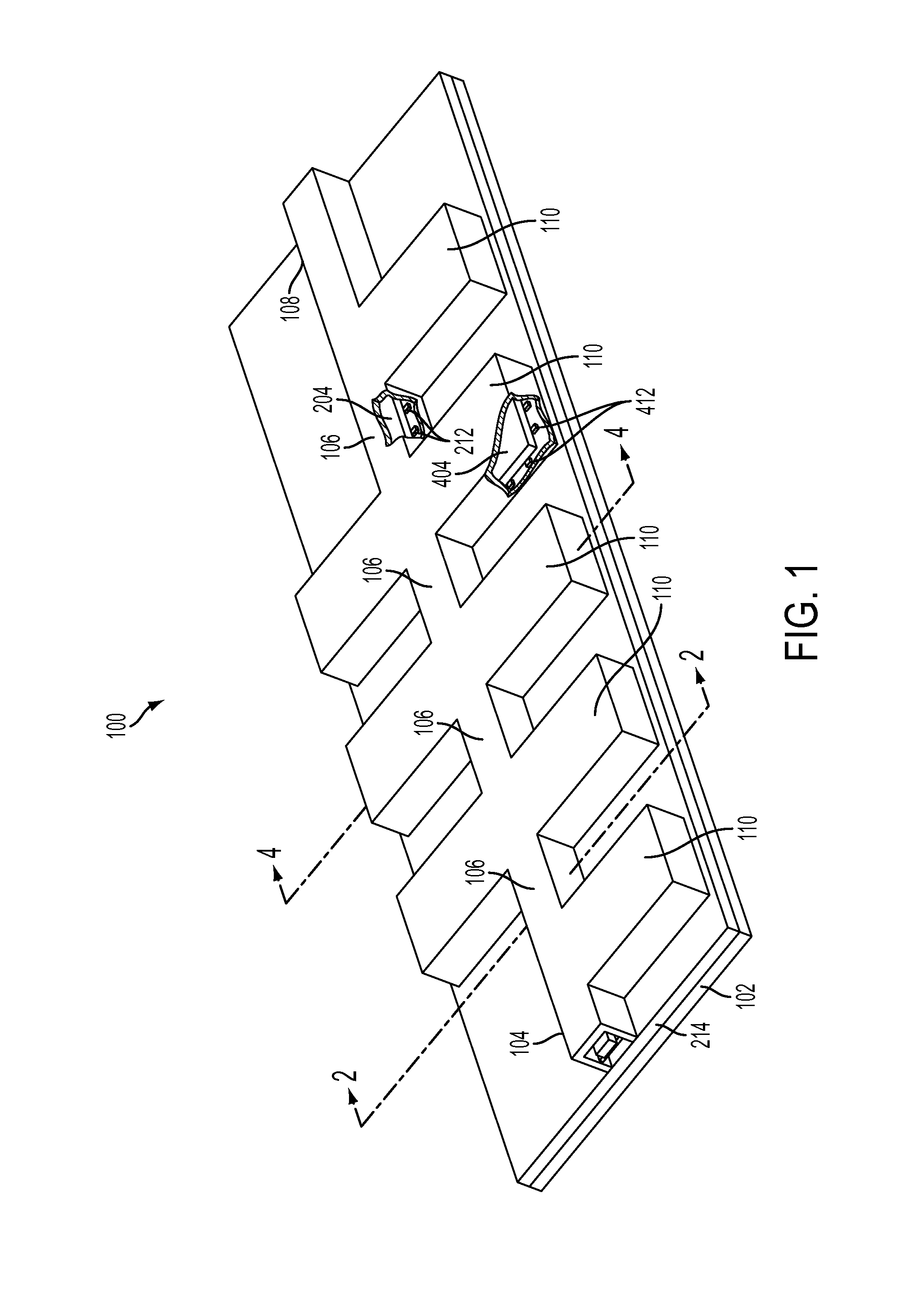
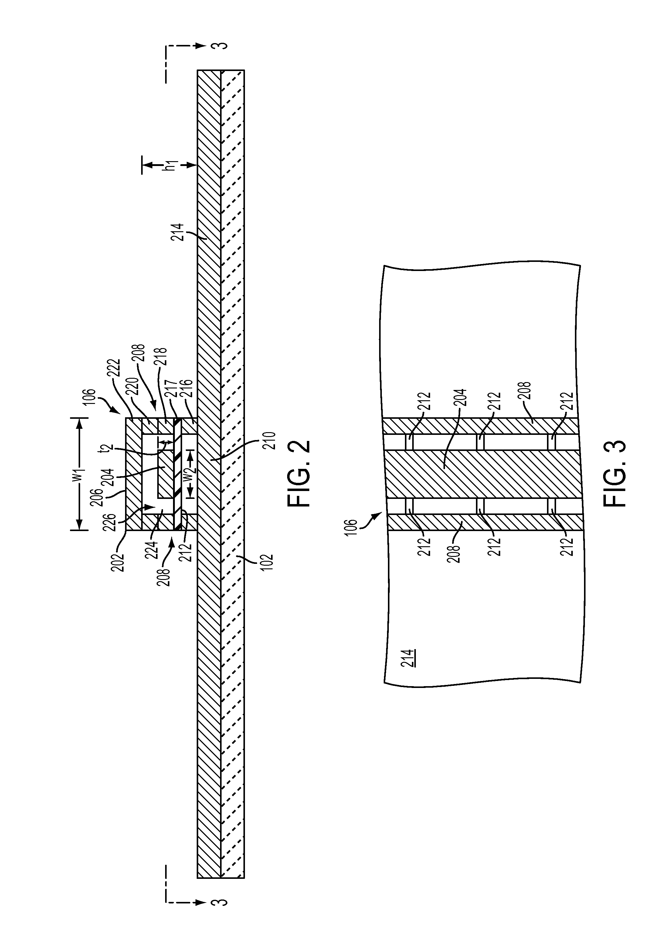
[0020]The invention is described with reference to the attached figures. The figures are not drawn to scale and they are provided merely to illustrate the instant invention. Several aspects of the invention are described below with reference to example applications for illustration. It should be understood that numerous specific details, relationships, and methods are set forth to provide a full understanding of the invention. One having ordinary skill in the relevant art, however, will readily recognize that the invention can be practiced without one or more of the specific details or with other methods. In other instances, well-known structures or operation are not shown in detail to avoid obscuring the invention. The invention is not limited by the illustrated ordering of acts or events, as some acts may occur in different orders and / or concurrently with other acts or events. Furthermore, not all illustrated acts or events are required to implement a methodology in accordance wit...


PUM


Abstract

A method for constructing a radio frequency filter (100) includes depositing on a dielectric substrate (102) a plurality of layers of a conductive material (210, 216, 218, 220, 222), a dielectric material (217), and a sacrificial material (1200, 1500, 1700, 1900). The deposition is controlled to form at least one transmission line (104, 106, 108) including a shield (202) and a center conductor (204) disposed coaxially within the shield. The deposition is further controlled to form at least one distributed filter element electrically coupled to the center conductor (204), and at least one housing (402) electrically coupled to the shield. The method also includes dissolving at least one layer of the sacrificial material to form an interior channel (226) within at least one shield. The dissolving of the sacrificial material also results in the formation of a interior space within at least one housing containing the distributed filter element.

Description

BACKGROUND OF THE INVENTION[0001]1. Statement of the Technical Field[0002]The inventive arrangements relate to filters for radio frequency signals, and more particularly to low loss filters formed of distributed filter elements.[0003]2. Description of the Related Art[0004]Communication systems, such as broadband satellite communications, commonly operate at extremely high frequencies. For example, communication systems operating at frequencies as high as 300 GHz are known. Filters are a necessary element in all communications system for passing desired signals and blocking other signals, e.g. noise. However, existing filters for high frequencies (e.g. 10 GHz to 300 GHz) are known to suffer from certain limitations. Conventional waveguide based filters for such frequencies have low insertion loss, but are very large in size (on the order of several inches in each dimension). Conversely, ceramic thin-film based filters can be relatively small in size but have low power handling capabi...

Claims


Application Information

Patent Timeline
Patent Type & Authority Applications(United States)
IPC IPC(8): H01P1/202B05D5/12
CPCH01P1/20336H01P1/20363
Inventor ROGERS, JOHN E.WEATHERSPOON, MICHAEL R.SMITH, DAVID M.
Owner HARRIS CORP
Why Eureka
Try Eureka