RF Switch with Adaptive Drain and Source Voltage

a technology of source voltage and rf switch, which is applied in the direction of electronic switching, electrical equipment, pulse technique, etc., can solve the problems of destroying the switching capability of rf switch, the inability of rf switch to isolate one path from the other, etc., and achieves the effect of increasing the permissible input signal amplitude and reducing the transient switching time of rf switch

Active Publication Date: 2014-03-06
RICHWAVE TECH CORP
View PDF2 Cites 19 Cited by
  • Summary
  • Abstract
  • Description
  • Claims
  • Application Information

AI Technical Summary

Benefits of technology

[0005]Embodiments of the present invention provide a radio frequency (RF) switch that includes a common port, a first port, and a second port. A first semiconductor switching element is disposed in a first RF pathway between the common port and the first port, and a second semiconductor switching element is disposed in a second RF pathway between the common port and the second port. A first pair of direct current (DC) blocking capacitors is disposed to isolate the first semiconductor switching element in the first RF pathway, and a second pair of DC blocking capacitors is disposed to isolate the second semiconductor switching element in the second RF pathway. The respective pairs of DC blocking capacitors

Problems solved by technology

When the power handling capability of an RF switch is low, the RF switch might not be able to isolate one path from another if the input signal is too great.
That is, the peak-to-peak voltage swing of an input signal might be sufficiently high to overcome the reverse

Method used


Image

  • RF Switch with Adaptive Drain and Source Voltage
  • RF Switch with Adaptive Drain and Source Voltage
  • RF Switch with Adaptive Drain and Source Voltage

Examples


Embodiment Construction

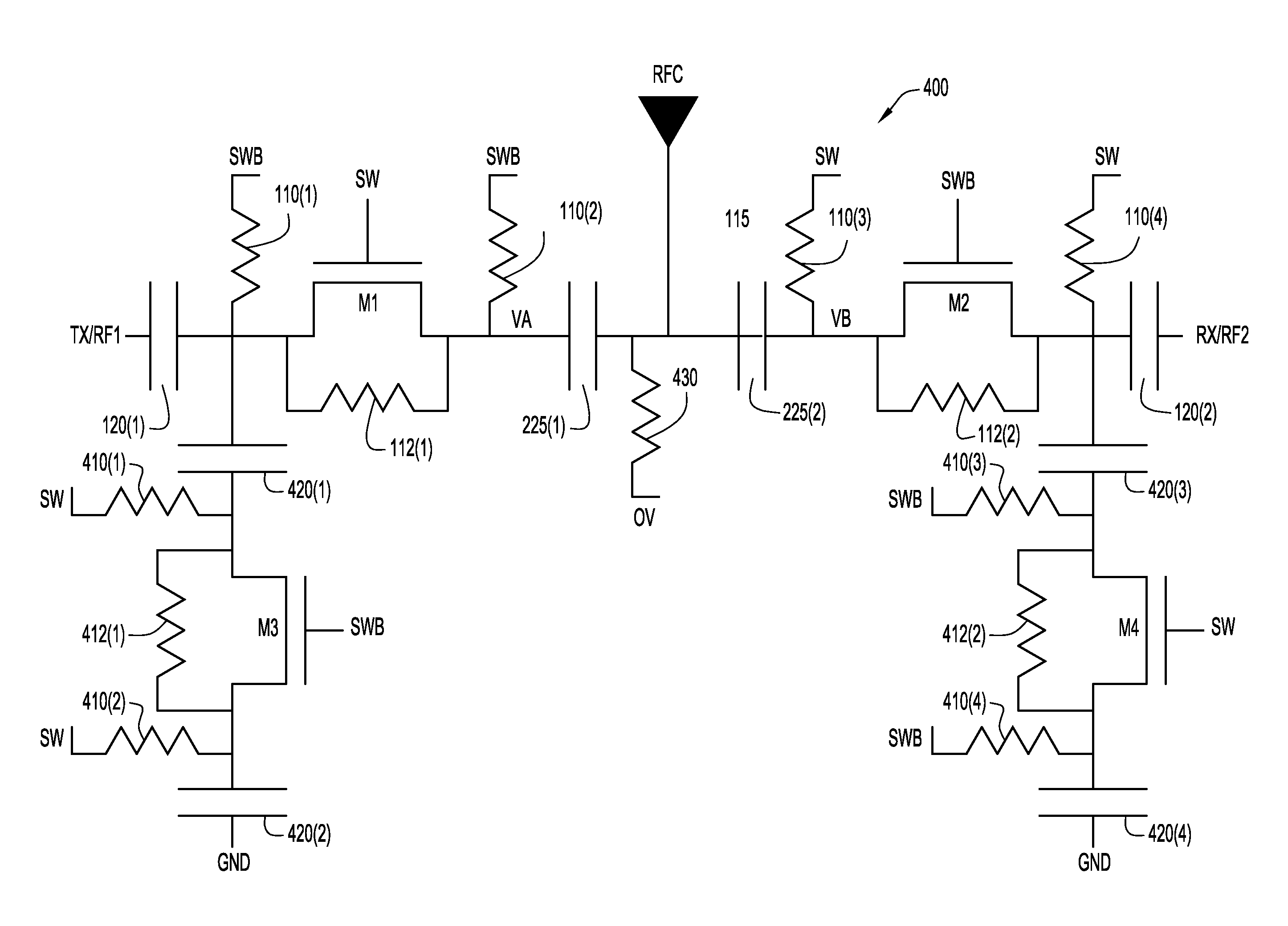
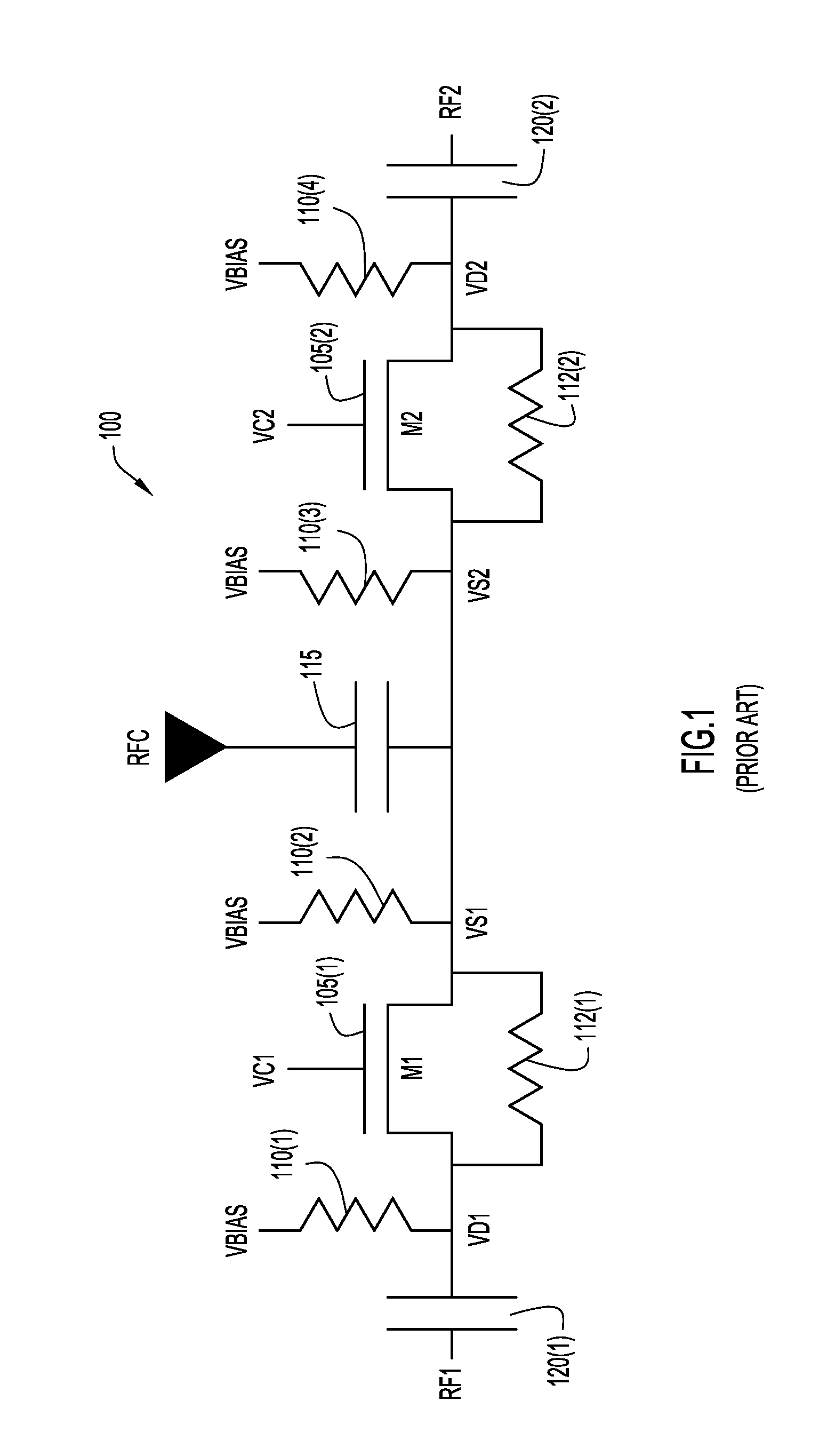
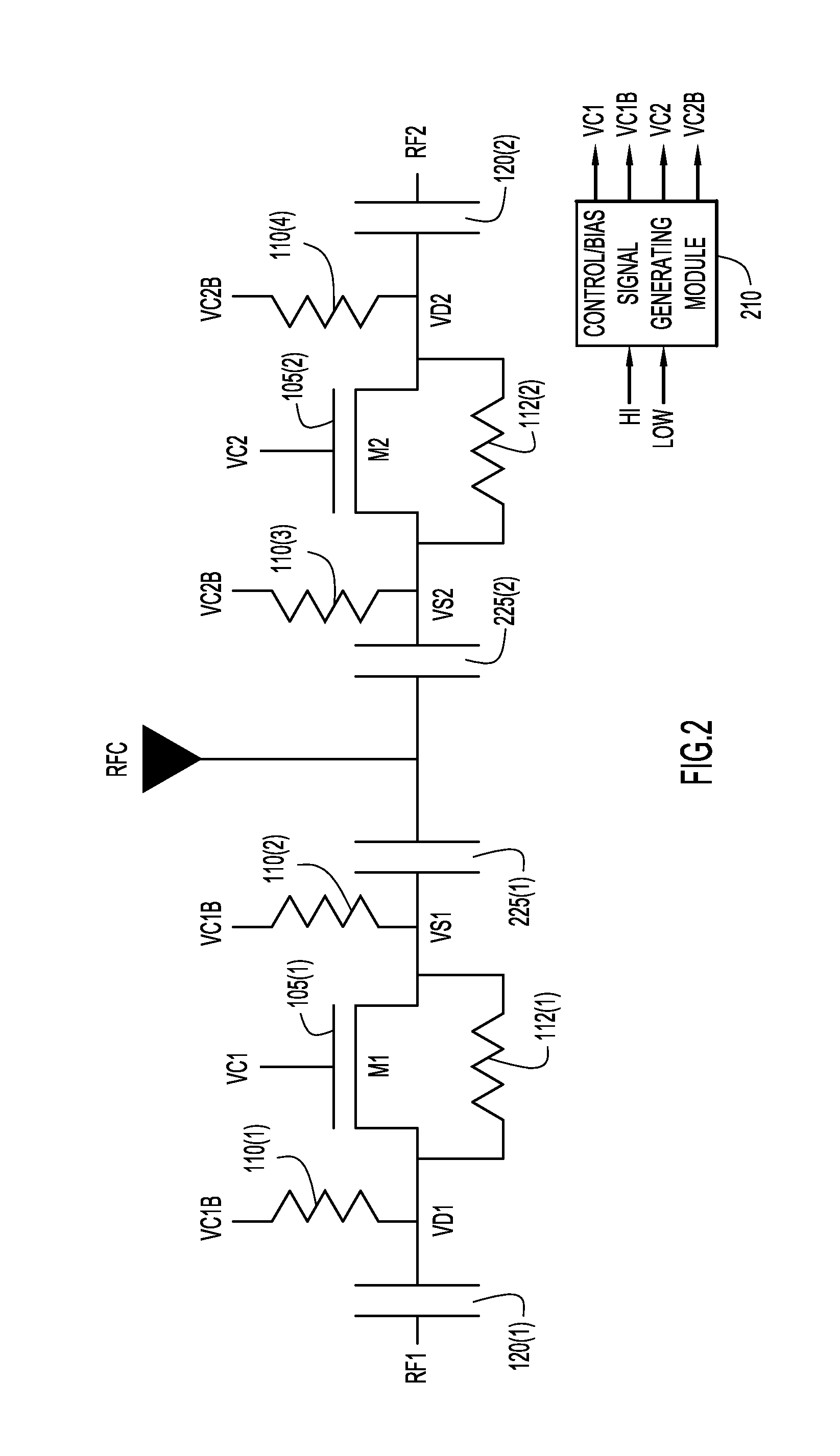
[0015]Reference is now made to FIG. 1, which depicts a conventional RF switch 100. RF switch 100 includes an RFC (radio frequency common) port, a first port RF1 and a second port RF2. A first semiconductor switching element M1 is disposed between RFC and first port RF1, and a second semiconductor switching element M2 is disposed between RFC and second port RF2. M1 and M2 may be, for example, MOSFET devices having respective source nodes (VS1, VS2), drain nodes (VD1, VD2) and gate control nodes (105(1), 105(2)). Although MOSFET devices are described herein as the semiconductor switching elements, the switching elements may alternatively comprise bipolar transistors among other semiconductor switching elements.

[0016]Resistors 110(1)-110(4) are connected to each of the source and drain nodes, and a bias voltage VBIAS is applied to the respective source and drain nodes. As will be explained below, VBIAS is a constant voltage, the application of which enables RF switch 100 to accommodate...


PUM


Abstract

A radio frequency (RF) switch includes a common port, a first port, and a second port, a first semiconductor switching element disposed in a first RF pathway between the common port and the first port, a second semiconductor switching element disposed in a second RF pathway between the common port and the second port, a first pair of direct current (DC) blocking capacitors disposed to isolate the first semiconductor switching element in the first RF pathway, and a second pair of DC blocking capacitors disposed to isolate the second semiconductor switching element in the second RF pathway. The respective pairs of DC blocking capacitors allow for different bias voltages to be applied to the respective RF pathways. A charge-discharge circuit may also be employed to decrease transient switching time of the RF switch.

Description

FIELD OF THE INVENTION[0001]The present invention relates to solid state radio frequency (RF) switches. More particularly, the present invention relates to an approach for biasing elements of an RF switch to achieve higher power handling capability and faster switching time.BACKGROUND OF THE INVENTION[0002]RF switches are important building blocks in many wired and wireless communication systems. Solid state RF switches are found in many different communication devices such as cellular telephones, wireless pagers, wireless infrastructure equipment, satellite communications equipment, and cable television equipment. As is well known, the performance of solid state RF switches may be characterized by one of any number operating performance parameters including insertion loss and switch isolation. Performance parameters are often tightly coupled, and any one parameter can be emphasized in the design of RF switch components at the expense of others. Other characteristics that are import...

Claims


Application Information

Patent Timeline
IPC IPC(8): H03K17/687
CPCH03K17/693
Inventor CHIH-SHENG, CHEN
Owner RICHWAVE TECH CORP
Why Eureka
Try Eureka