Contact protection for integrated circuit device loading

a technology for integrated circuit devices and contact protection, which is applied in the direction of electrical apparatus construction details, printed circuit non-printed electric components association, and semiconductor/solid-state device details, etc., can solve the problems of inconvenient and easy damage of contacts, large amount of heat generated by integrated circuit packages, and relatively small contacts, etc. problem, to achieve the effect of ensuring the proper alignment between the contacts of the integrated circuit package and the sock

Active Publication Date: 2014-04-03
INTEL CORP
View PDF11 Cites 10 Cited by
  • Summary
  • Abstract
  • Description
  • Claims
  • Application Information

AI Technical Summary

Problems solved by technology

Integrated circuit packages frequently generate a large amount of heat.
Accordingly, the contacts tend to be relatively small and therefore relatively fragile and susceptible to damage, particularly when the integrated circuit package is installed in the socket by hand.
Hence, proper alignment between the contacts of the integrated circuit package and the socket is frequently a challenge.

Method used


Image

  • Contact protection for integrated circuit device loading
  • Contact protection for integrated circuit device loading
  • Contact protection for integrated circuit device loading

Examples


embodiment details

Additional Embodiment Details

[0060]In certain embodiments, the stack embodiments may be embodied in a computer system including a video controller to render information to display on a monitor coupled to a computer system comprising a desktop, workstation, server, mainframe, laptop, handheld computer, etc. Alternatively, the stack embodiments may be embodied in a computing device that does not include a video controller, such as a switch, router, etc.

[0061]The illustrated operations of FIG. 8 show certain events occurring in a certain order. In alternative embodiments, certain operations may be performed in a different order, modified or removed. Moreover, operations may be added to the above described operations and still conform to the described embodiments. Further, operations described herein may occur sequentially or certain operations may be processed in parallel.

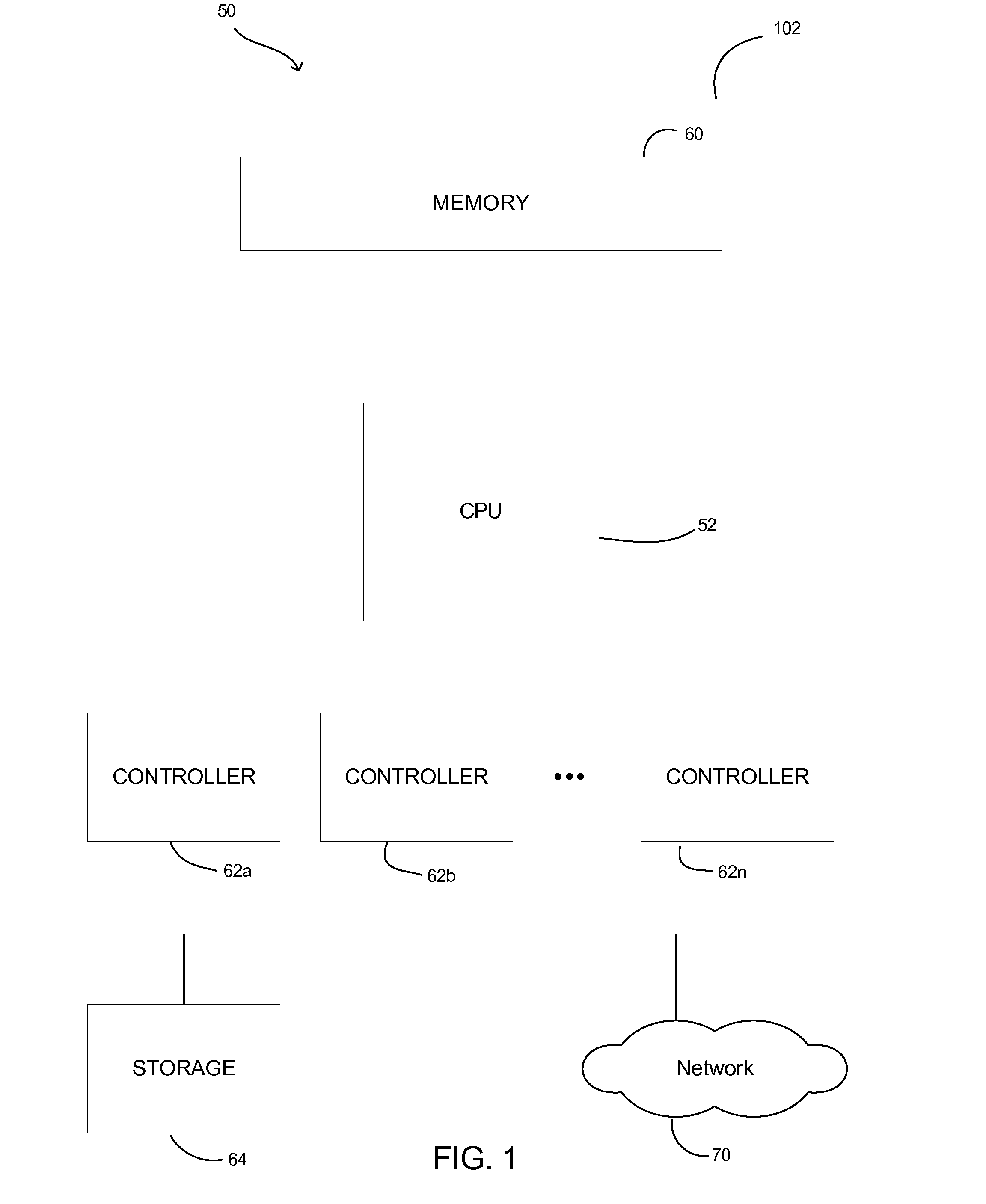
[0062]FIG. 11 illustrates one embodiment of a computer architecture 700 which can utilize components, such the devi...


PUM


Abstract

In one embodiment, a load frame and an integrated circuit device are aligned, with a base frame carried on a substrate, along a first alignment axis defined by a first alignment post extending from the base frame to the load frame, in a direction transverse to the substrate, and a first biasing device carried on the base frame is actuated to engage and bias the load frame toward the base frame aligned with the load frame, and to bias the integrated circuit toward the substrate. A latch latches the load and base frames together, aligned with and biased towards each other with the integrated circuit device and the substrate aligned with, and biased toward each other. Other aspects and features are also described.

Description

BACKGROUNDDescription of Related Art[0001]Integrated circuits typically include various active and passive circuit elements which have been integrated into a piece of semiconductor material, often referred to as a die. The die may, in turn, be encapsulated into a package, which often includes a ceramic or plastic substrate although other materials may be used. These packages are usually physically attached to a printed circuit board or other substrate.[0002]Integrated circuit packages frequently generate a large amount of heat. Accordingly, the larger integrated circuit packages for large integrated circuits such as processors typically have a thermal device such as a heat sink installed on an outer surface of the integrated circuit package to draw heat energy from the integrated circuit package to cool the integrated circuits of the package.[0003]Printed circuit boards frequently include a socket or other receptacle in which the integrated circuit package is inserted. The socket ty...

Claims


Application Information

Patent Timeline
Patent Type & Authority Applications(United States)
IPC IPC(8): H05K1/18H01L23/544H01L21/02
CPCH05K3/301H05K7/1007H05K7/1061H05K2201/10325H05K2201/2018H05K2203/167
Inventor LLAPITAN, DAVID J.ULEN, NEAL E.SMALLEY, JEFFORY L.
Owner INTEL CORP
Why Eureka
Try Eureka