Testing method and testing system for semiconductor element

Active Publication Date: 2014-04-17
IND TECH RES INST
View PDF11 Cites 6 Cited by
  • Summary
  • Abstract
  • Description
  • Claims
  • Application Information

AI Technical Summary

Benefits of technology

The invention provides a testing method for a semiconductor element to detect its tolerance to electrostatic discharge (ESD). The method involves applying a testing ESD voltage to the semiconductor element and measuring its ESD decay rate. The method also includes measuring a basic characteristic offset of the semiconductor element to obtain its relation with the testing ESD voltage. The system for implementing this method includes an electrostatic generator, a current probe, and a determination device. The non-destructive testing method allows for comprehensive testing of all semiconductor elements on ESD tolerance.

Problems solved by technology

Damage caused by ESD is the most common reason that causes failure of the semiconductor elements, which is easy to cause severe damage of application products.
A general testing method for ESD tolerance of a semiconductor element is limited to a destructive testing method.
The destructive testing method is to impose gradually increased ESD voltages to the semiconductor element to impact the tested semiconductor element until it fails, so as to detect a limit of the tested semiconductor element for the ESD tolerance.
However, since the ESD testing method is destructive, it is easy to cause detriment to the semiconductor elements, so that samples are selected by sample inspection to represent all of the elements, by which a manufacturer cannot conduct a comprehensive test on the ESD tolerance to achieve a purpose of grading the manufactured products, which directly influences reliability of the products and a benefit of price differentiation.
Therefore, how to resolve the problem that the manufacturer cannot, conducting a comprehensive testing on the ESD tolerance to achieve the purpose of grading the manufactured products through a non-destructive testing method for ESD tolerance, becomes an issue worthy of further exploration.

Method used


Image

  • Testing method and testing system for semiconductor element
  • Testing method and testing system for semiconductor element
  • Testing method and testing system for semiconductor element

Examples


Embodiment Construction

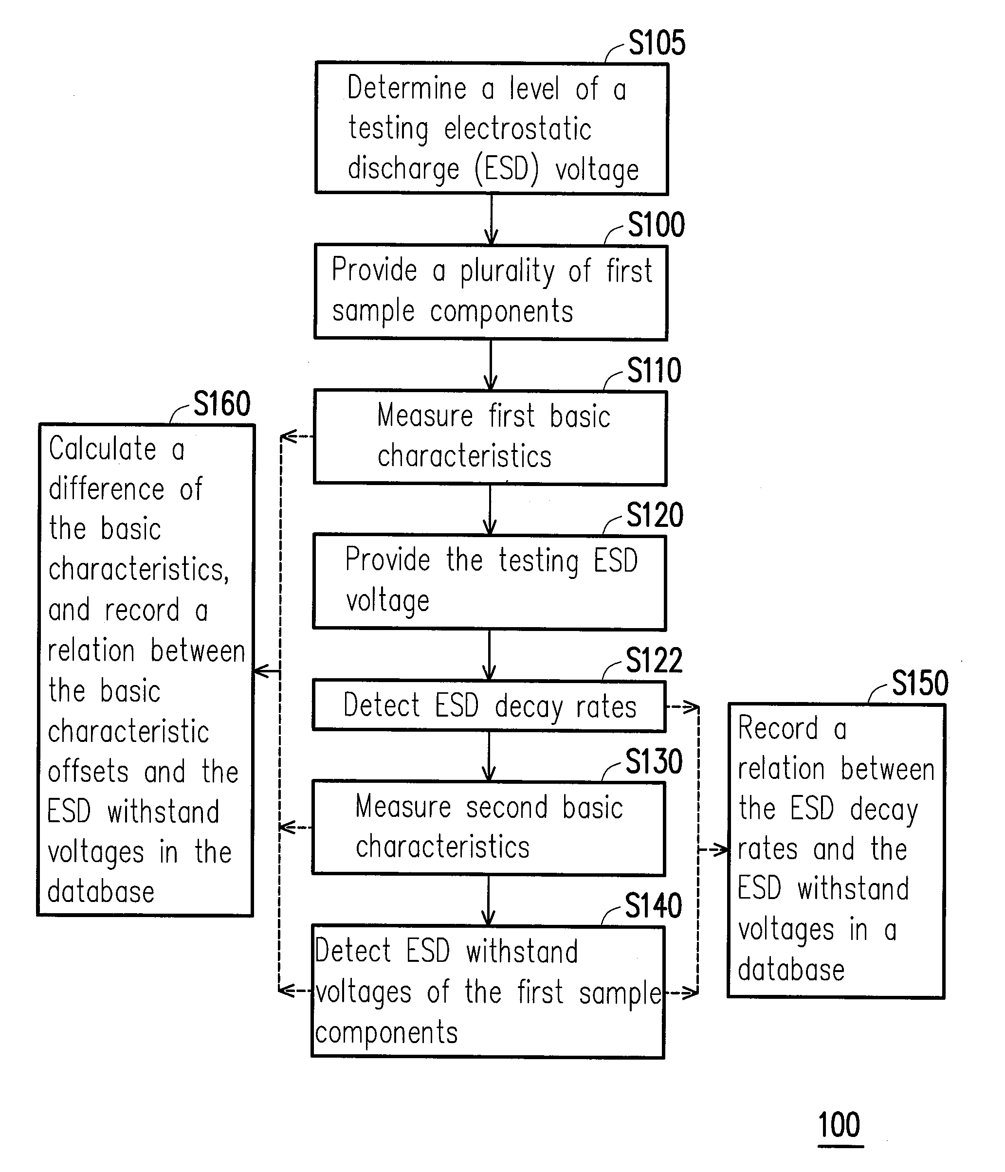
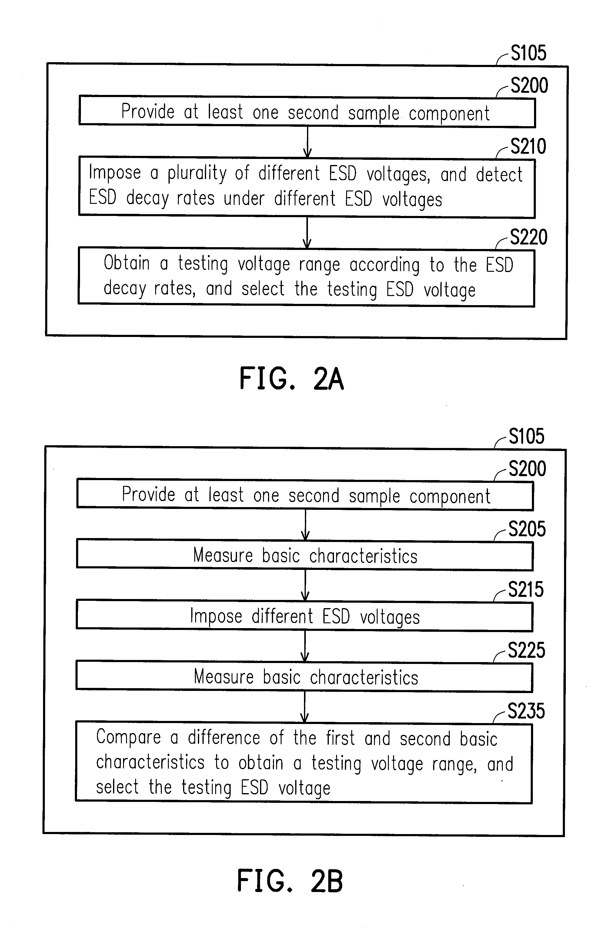
[0025]Referring to FIG. 10 first, FIG. 10 is a flowchart illustrating a testing method for a semiconductor element according to an embodiment of the disclosure. Referring to FIG. 10, a semiconductor electrostatic discharge (ESD) testing method 1000 mainly includes a pre-testing method 100 and a general testing method 200. In the pre-testing method 100, by detecting an ESD decay rate of the semiconductor element, and / or by detecting relations between a current-voltage characteristic variation and an ESD withstand voltage of the semiconductor element before and after the ESD, a plurality of batches of relation data is used to establish a database. The general testing method 200 is used to look up the database to determine the ESD withstand voltage of the semiconductor element. Steps of the pre-testing method 100 and the general testing method200 are described in detail later.

[0026]FIG. 1 is a flowchart illustrating an ESD pre-testing method for a semiconductor element of FIG. 10 accor...


PUM


Abstract

A testing method and testing system for a semiconductor element are provided. The method includes following steps. A level of a testing electrostatic discharge (ESD) voltage is determined. A plurality of sample components is provided. The testing ESD voltage is imposed on the sample components for testing ESD decay rates of the sample components. ESD withstand voltages of the sample components are detected. The relation between the ESD withstand voltages and the electrostatic discharge rates are recorded to a database. The testing ESD voltage is imposed on the semiconductor element for testing an ESD decay rate of the semiconductor element. The database is looked up according to the ESD decay rate of the semiconductor element to determine an ESD withstand voltage of the semiconductor element.

Description

CROSS-REFERENCE TO RELATED APPLICATION[0001]This application claims the priority benefit of Taiwan application serial no. 101137506, filed on Oct. 11, 2012. The entirety of the above-mentioned patent application is hereby incorporated by reference herein and made a part of this specification.BACKGROUND[0002]1. Technical Field[0003]The disclosure relates to a testing for a semiconductor element. Particularly, the disclosure relates to a testing method for semiconductor electrostatic discharge (ESD) tolerance and a testing system thereof.[0004]2. Related Art[0005]Damage caused by ESD is the most common reason that causes failure of the semiconductor elements, which is easy to cause severe damage of application products.[0006]A general testing method for ESD tolerance of a semiconductor element is limited to a destructive testing method. The destructive testing method is to impose gradually increased ESD voltages to the semiconductor element to impact the tested semiconductor element u...

Claims


Application Information

Patent Timeline
IPC IPC(8): G01R31/26
CPCG01R31/2603G01R31/2644G01R31/001G01R31/275
Inventor CHEN, TZUNG-TEDAI, CHUN-FANFU, HAN-KUEIWANG, CHIEN-PINGCHOU, PEI-TING
Owner IND TECH RES INST
Why Eureka
Try Eureka