Electroluminescence display device
a display device and electroluminescent technology, applied in the direction of basic electric elements, semiconductor devices, electrical equipment, etc., to achieve the effect of improving the reliability of the color purity of the light emission by the el display devi
- Summary
- Abstract
- Description
- Claims
- Application Information
AI Technical Summary
Benefits of technology
Problems solved by technology
Method used
Image

Examples
first embodiment
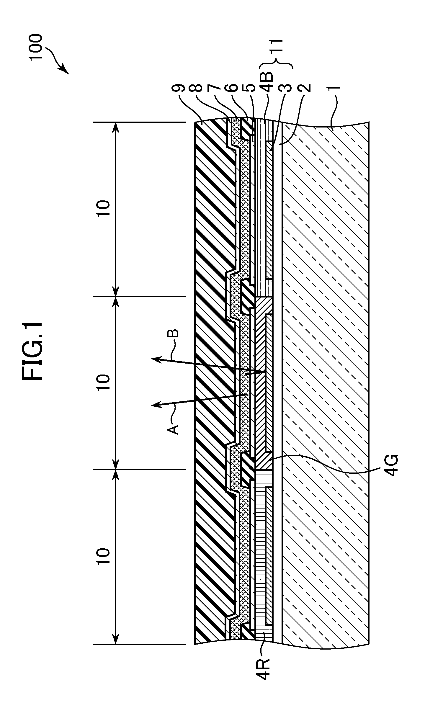
[0046]FIG. 1 is a schematic cross-sectional view illustrating a pixel portion of an EL display device 100 according to a first embodiment of the present invention.
[0047]The EL display device 100 regularly arranges a large number of pixels 10 on an insulating first substrate 1, and controls the amount of light emission of an EL layer 7 at a position corresponding to each pixel 10 to form an image. For that reason, a circuit layer 2 in which electric circuits including TFTs (thin film transistors) for controlling the amount of current flowing in the respective pixels 10 are regularly (in a lattice pattern in this embodiment) arranged is formed on the first substrate 1. The first substrate 1 is formed of a glass substrate in this embodiment, but a material of the first substrate 1 is not particularly limited if the substrate is made of an insulating material. The first substrate 1 may be made of synthetic resin or other material. Also, the first substrate 1 maybe transparent or opaque....
second embodiment
[0066]On the contrary, in an EL display device 200 according to a second embodiment of the present invention illustrated in FIG. 3, the color selection reflection layer 11 is formed of a single layer. FIG. 3 is a schematic cross-sectional view illustrating a pixel portion of the EL display device 200 according to the second embodiment of the present invention. In this embodiment, parts common to those in the above first embodiment are denoted by the same symbols, and a repetitive description will be omitted.
[0067]In the EL display device 200, dichroic mirror layers 12R, 12G, and 12B are disposed as the color selection reflection layer 11. The dichroic mirror layer 12R has a property of selectively reflecting only red color, and transmitting the other lights. The dichroic mirror layers 12G and 12B also reflect green light and blue light, respectively. In this embodiment, the light beams that have been transmitted through the dichroic mirror layers 12R, 12G, and 12B arrive at the circ...
third embodiment
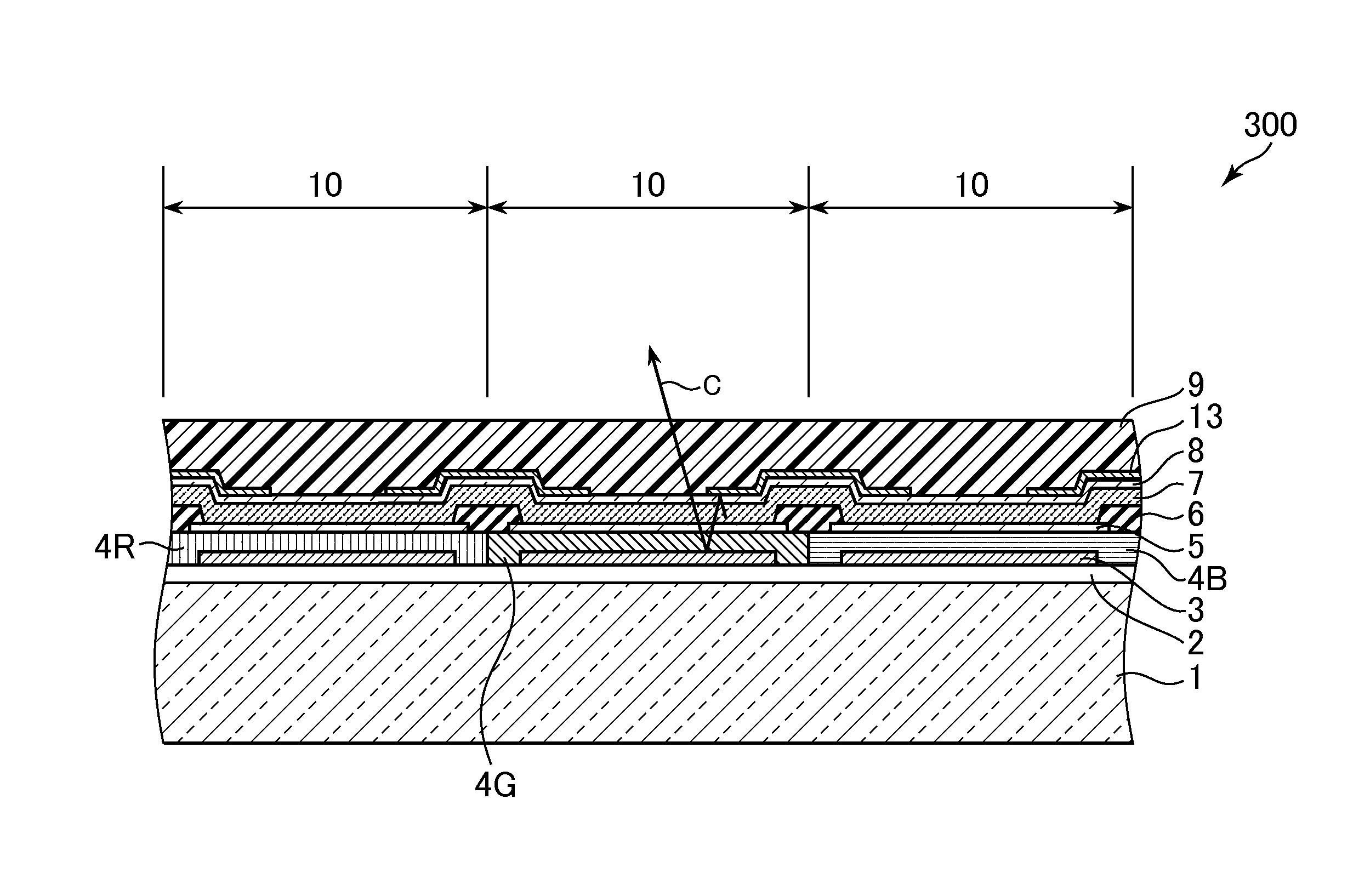
[0070]In an EL display device 300 according to a third embodiment of the present invention illustrated in FIG. 4, a reflection layer that covers a part of the aperture area of the pixels 10 is formed in the upper layer of the upper electrode 8. FIG. 4 is a schematic cross-sectional view illustrating a pixel portion of the EL display device 300 according to the third embodiment of the present invention. In this embodiment, parts common to those in the above first embodiment are denoted by the same symbols, and a repetitive description will be omitted.
[0071]In the EL display device 300 according to this embodiment, an auxiliary electrode 13 is disposed in the upper layer of the upper electrode 8, and immediately above the pixel separation films 6. The auxiliary electrode 13 is formed of a conductive metal film made of silver or aluminum, and small in electric resistance. Therefore, the auxiliary electrode 13 has a function of keeping a uniform potential of the overall upper electrode ...
PUM
 Abstract
Description
Claims
Application Information
 - R&D Engineer
- R&D Manager
- IP Professional
- Industry Leading Data Capabilities
- Powerful AI technology
- Patent DNA Extraction
Browse by: Latest US Patents, China's latest patents, Technical Efficacy Thesaurus, Application Domain, Technology Topic.
© 2024 PatSnap. All rights reserved.Legal|Privacy policy|Modern Slavery Act Transparency Statement|Sitemap