Wavelength-converting converter material, light-emitting optical component, and method for the production thereof
- Summary
- Abstract
- Description
- Claims
- Application Information
AI Technical Summary
Benefits of technology
Problems solved by technology
Method used
Image
Examples
Embodiment Construction
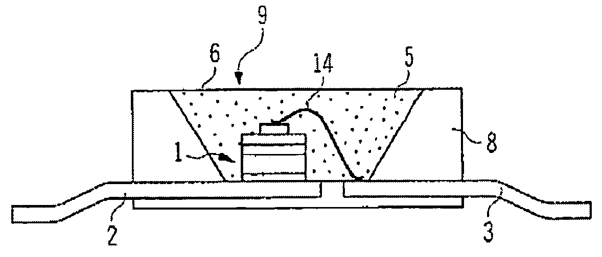
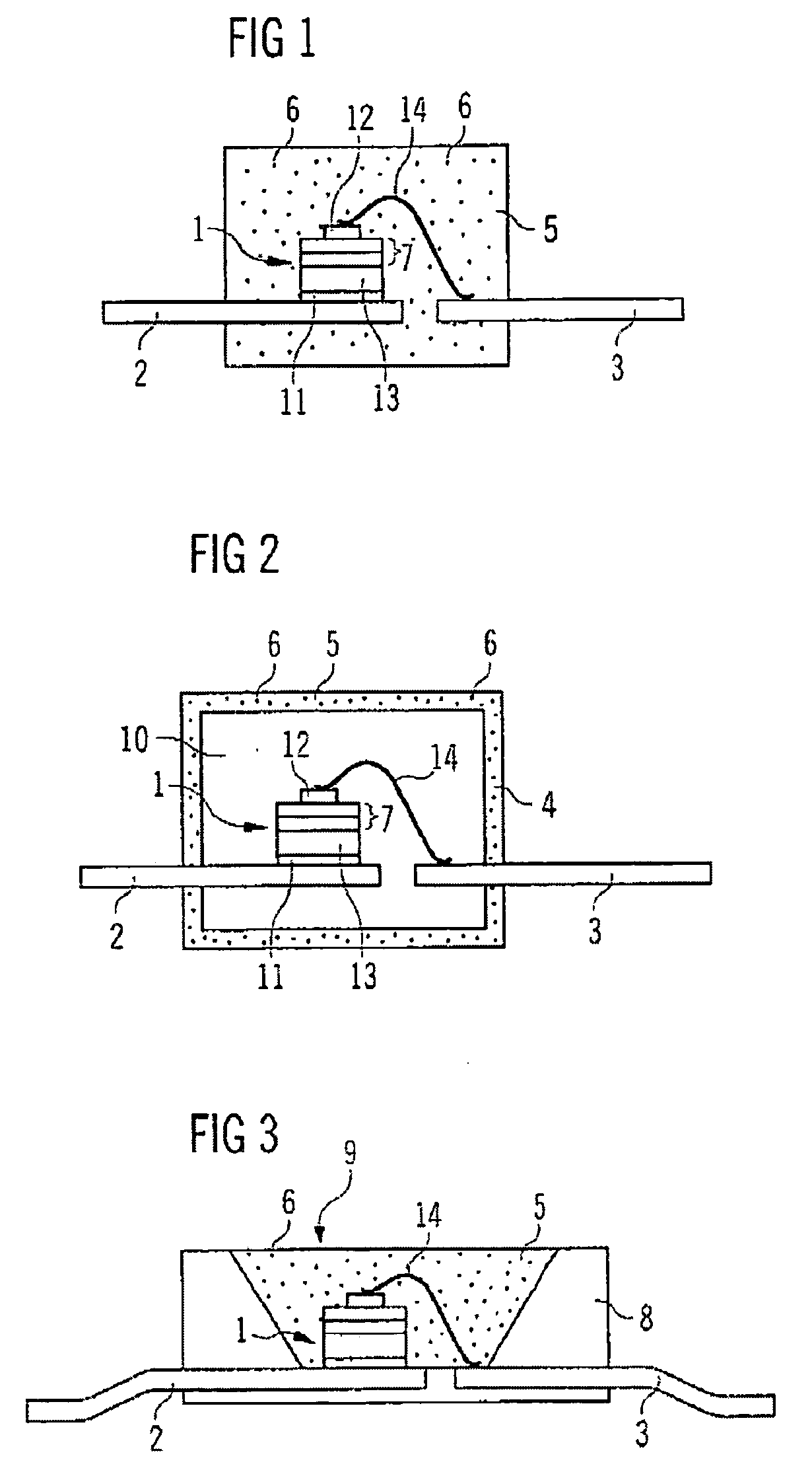
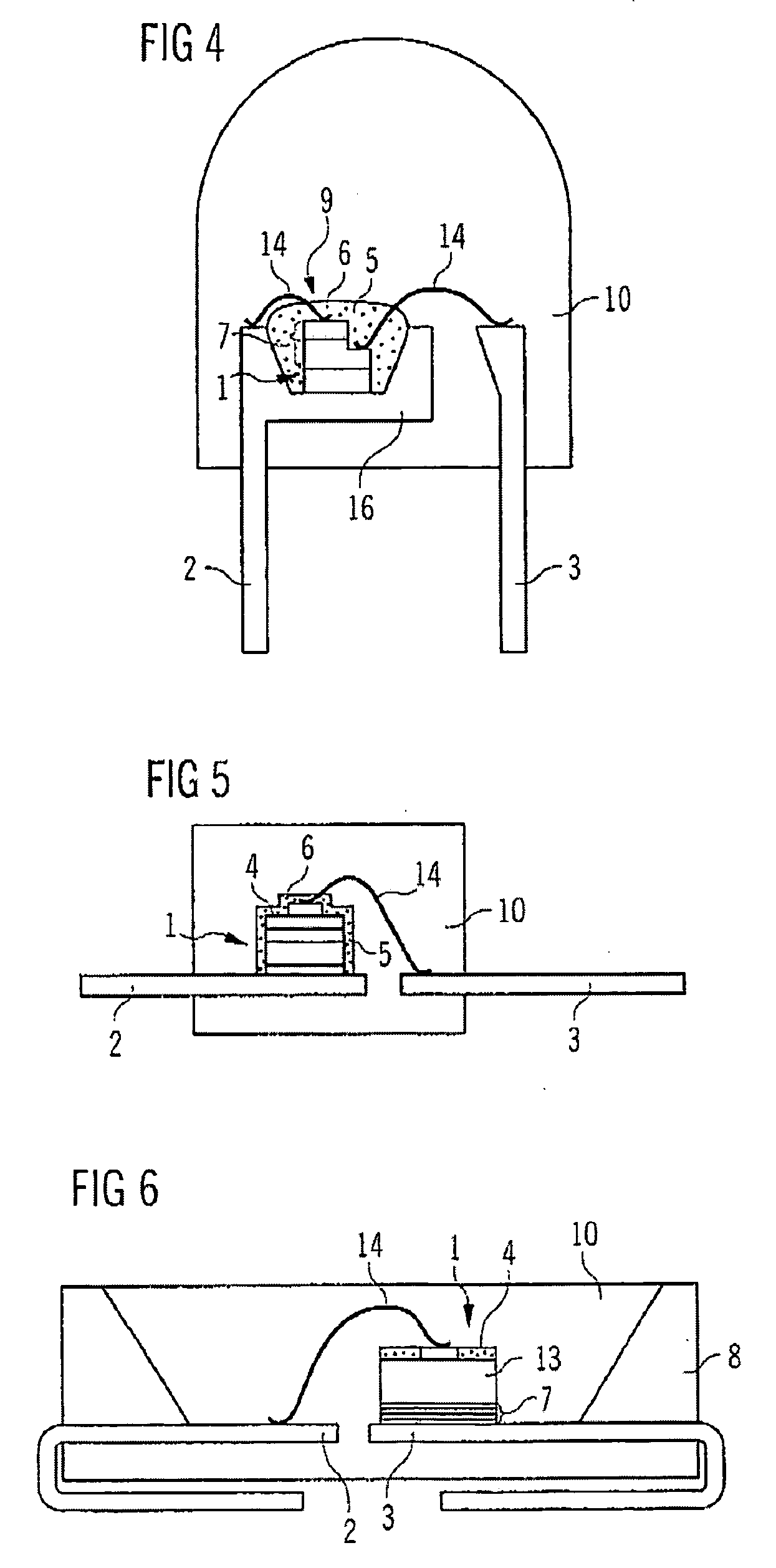
[0074]The light-emitting semiconductor component of FIG. 1 comprises a wavelength-converting converter material according to the invention. This contains at least one transparent, i.e. radiation-pervious, preferably non-yellowing and particularly hydrolysis- and temperature-resistant polymer.
[0075]The component comprises a semiconductor body 1, e.g. an LED chip. This is attached by its rear-side contact 11 to a first electrical lead 2 of a leadframe via an electrically conductive connecting means 7.
[0076]The semiconductor body 1 comprises an active layer or layer sequence 7 having one layer or a plurality of layers based on InxGayAl1-x-yN, where 0≦x≦1,0≦y≦1 and x+y≦1. The layer or layer sequence 7 has, for example, a multi-quantum well structure. The LED chip includes, for example, a substrate 13. Alternatively, it can also be free of substrate.
[0077]Used as the electrical connecting means is, for example, a metallic solder, particularly soft solder, or a glue. The front-side contac...
PUM
| Property | Measurement | Unit |
|---|---|---|
| Length | aaaaa | aaaaa |
| Length | aaaaa | aaaaa |
| Length | aaaaa | aaaaa |
Abstract
Description
Claims
Application Information


