

Pixel control element selection transfer method, pixel control device mounting device used for pixel control element selection transfer method, wiring formation method after pixel control element transfer, and planar display substrate
a technology of pixel control element and mounting device, which is applied in the direction of radiation control device, identification means, instruments, etc., can solve the problems of cvd device etc., planar display substrate, having to be inevitably enlarged, and difficult to reduce fabrication cost, etc., to achieve the effect of stable formation
- Summary
- Abstract
- Description
- Claims
- Application Information
AI Technical Summary
Benefits of technology
Problems solved by technology
Method used
Image

Examples
first embodiment
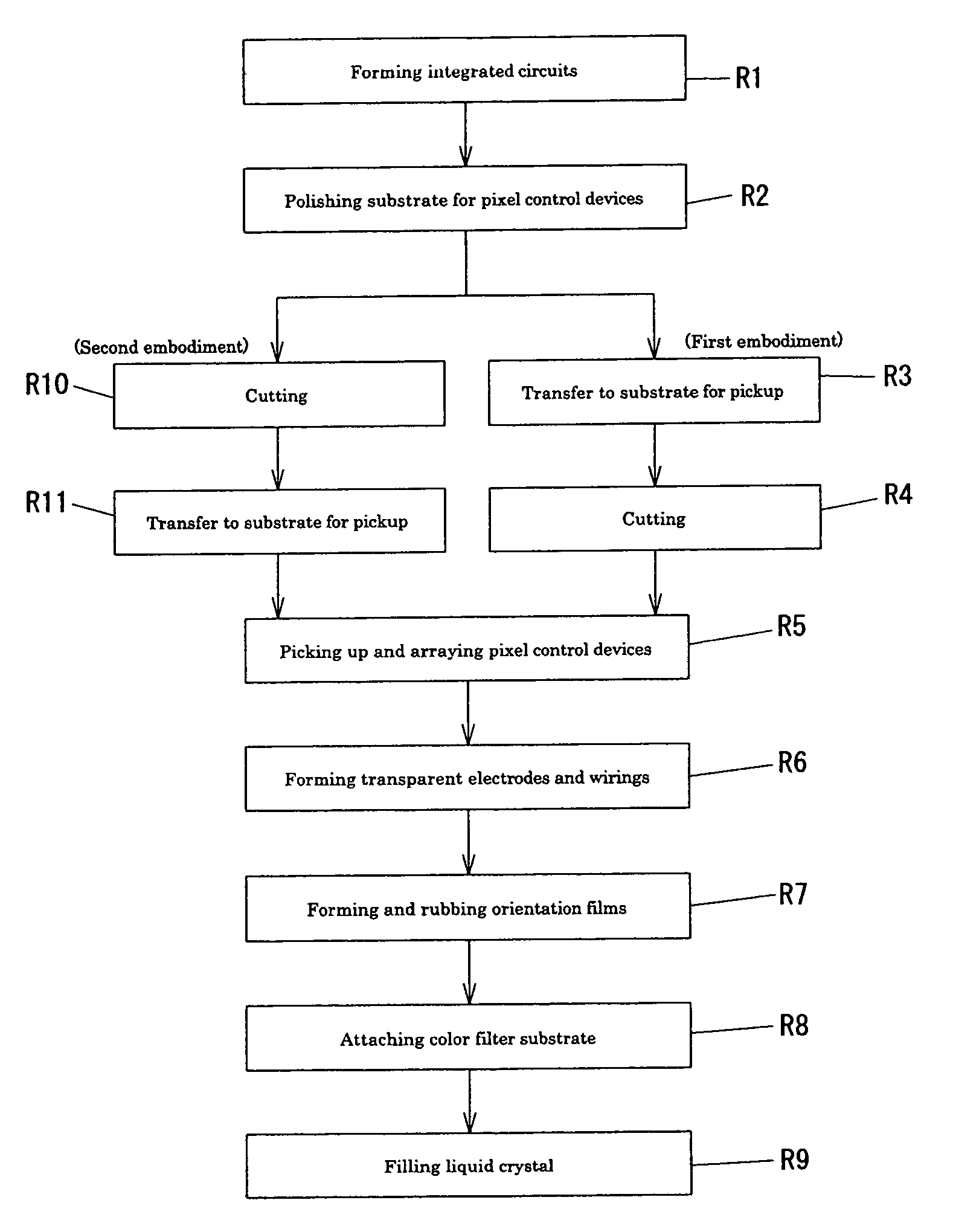
METHOD OF PRODUCING A PLANAR DISPLAY SUBSTRATE
[0088](1. Structure of a Liquid Crystal Display)
[0089]In the present embodiment, a method for producing a planar display substrate according to the present invention is applied to the production of a liquid crystal display. A liquid crystal display 200 has a structure, as shown in FIG. 24, comprising a planar display substrate 100, a color filter substrate 111 and a liquid crystal 112 interposed between them. The planar display substrate of plastic (also called the first substrate or array substrate) 100 has a pixel control device 1 and transparent electrodes (pixels) 102 formed thereon via a resin film 101 in matrix form on which an orientation film 110 is formed. On the other hand, the color filter substrate 111 has a color filter 114 formed thereon via a solvent resistant layer 113 so that the color filter is opposed to the transparent electrodes 102. On the surface of the solvent resistant layer, a transparent electrode for color fil...
second embodiment
METHOD OF PRODUCING A PLANAR DISPLAY SUBSTRATE
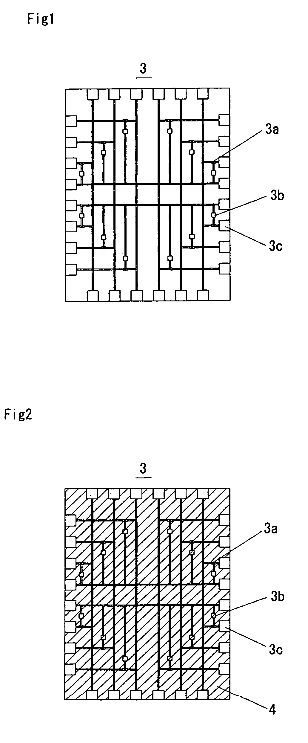
[0114]In the present embodiment, a transfer step R11 to the substrate 9 for pickup is performed as shown in the flow chart of FIG. 25 after the cutting step R10 for pixel control devices 1. After the mechanical polishing of the silicon substrate 2 shown in FIG. 6 at step R2, positional alignment of the integrated circuits 3 formed on the silicon substrate 2 and patterning of the pixel control devices 1 are conducted so that cutting can be established at step 10 between the integrated circuits 3. At this time, since the integrated circuits 3 exist not on the side of the front surface of the silicon substrate 1, but on the side in contact with the support substrate 7, the positional alignment cannot be conducted while discernibly confirming the positions thereof directly from above. Therefore, the positional alignment can be conducted through provision of position-aligning marks on the back surface 2b of the silicon substrate 2 or formatio...
example
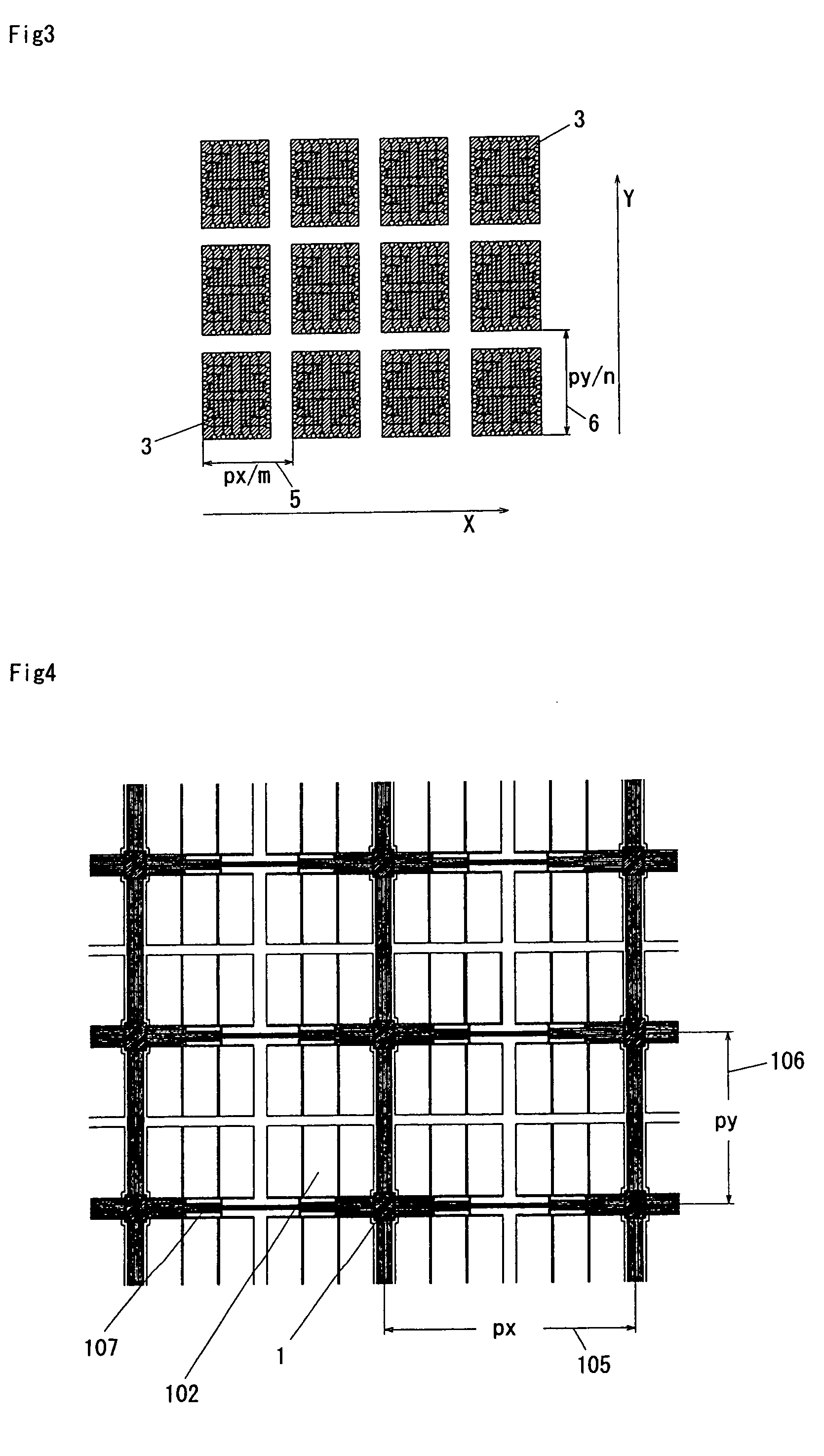
[0134]An actual example will be described, in which the mounting apparatus 300 is used to selectively transfer pixel control devices 1 onto a planar display substrate 100 for a liquid crystal display. The liquid crystal display has a diagonal dimension of 50 inches and a screen resolution of SXGA. When producing pixel control devices 1 having a longitudinal size of 200 μm, a lateral size of 150 μm and a thickness of 0.06 mm at a pitch 5 of 0.215 mm in the first direction X and a pitch 6 of 0.244 mm in the second direction Y on a 8-inch silicon substrate 2 (200 mm in diameter), 370,000 pixel control devices 1 per silicon substrate (having a device formation portion of 140 mm×140 mm) can be produced. When a liquid crystal display 200 having a diagonal dimension of 50 inches (1107 mm×623 mm) and a screen resolution of SXGA (1280×1024×3 colors) is to be produced, one pixel (3 colors) measures 0.86 mm×0.61 mm. That is to say, the pitch 105 of the pixel control devices 1 on the planar dis...
PUM
| Property | Measurement | Unit |
|---|---|---|
| temperature | aaaaa | aaaaa |
| thickness | aaaaa | aaaaa |
| thickness | aaaaa | aaaaa |
Abstract
Description
Claims
Application Information