Eureka AIR delivers breakthrough ideas for toughest innovation challenges, trusted by R&D personnel around the world.

Semiconductor device and method of manufacturing semiconductor device

Inactive Publication Date: 2014-05-08
AMKOR TECH INC DW US
View PDF38 Cites 171 Cited by
  • Summary
  • Abstract
  • Description
  • Claims
  • Application Information

AI Technical Summary

Benefits of technology

The patent describes a semiconductor device and a method to manufacture it. The device has certain features that provide technical benefits, such as improved performance or reliability. The method of manufacturing the device ensures that it is produced efficiently and accurately. These technical effects can benefit various industries and applications that use the semiconductor device.

Problems solved by technology

In such an arrangement, the semiconductor package is formed of a plurality of stacked semiconductor die, and if one semiconductor die is defective, the remaining stacked semiconductor die become useless.
Accordingly, the cost of the loss of the entire semiconductor package and its semiconductor die occurs.

Method used


Image

  • Semiconductor device and method of manufacturing semiconductor device
  • Semiconductor device and method of manufacturing semiconductor device
  • Semiconductor device and method of manufacturing semiconductor device

Examples


Embodiment Construction

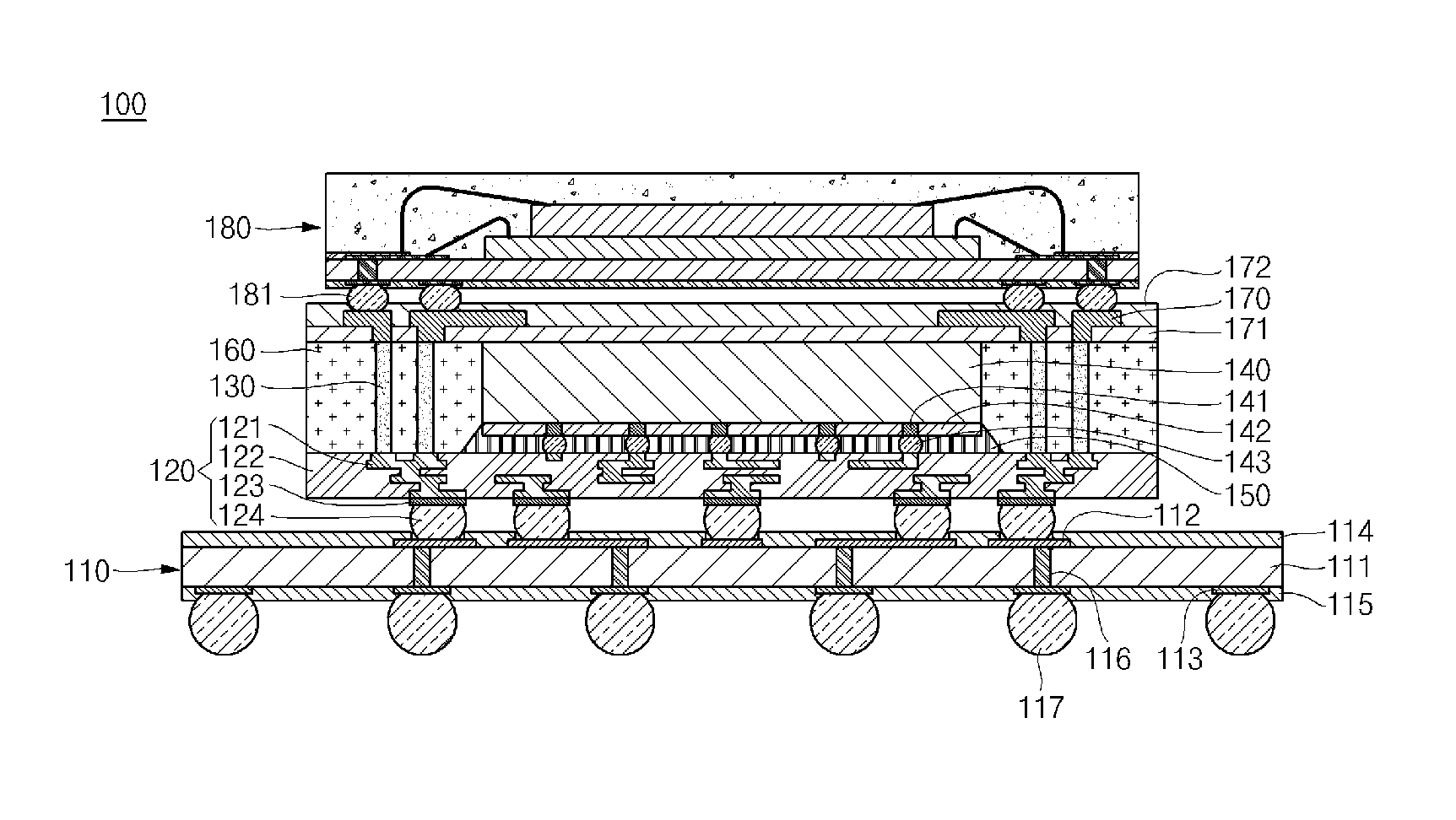
[0013]Aspects of the present invention relate to a semiconductor device and a method of manufacturing the same. More specifically, representative embodiments of the present invention may relate to a semiconductor device and a method of manufacturing such a semiconductor device, where the semiconductor device includes a plurality of semiconductor die, in which the manner of manufacture reduces costs by preventing the loss of other semiconductor die due to one or more defective semiconductor die.

[0014]Various aspects of the invention will be described in more detail with reference to the accompanying drawings. In such a manner, those skilled in the art will easily realize various aspects of the present invention upon reading the present patent application.

[0015]It should be noted that the thickness or size of each layer may be exaggerated for clarity in the accompanying drawings, and that like reference numerals may refer to like elements. Additionally, the term “semiconductor die” in...


PUM


Abstract

Provided are a semiconductor device and a method of manufacturing the same. The method may, for example, comprise forming an interposer on a dummy substrate; forming a conductive pillar on the interposer; contacting the top of the interposer with at least one semiconductor die; encapsulating the conductive pillar and the at least one semiconductor die with an encapsulant; forming a redistribution layer that is electrically connected to the conductive pillar, on the semiconductor die; removing the dummy substrate from the interposer; attaching the interposer, which has the at least one semiconductor die in contact, to a substrate and testing the at least one semiconductor die; and contacting a stacked semiconductor device with the redistribution layer.

Description

CROSS-REFERENCE TO RELATED APPLICATIONS / INCORPORATION BY REFERENCE[0001]The present application makes reference to, claims priority to, and claims the benefit of Korean Patent Application No. 10-2012-0125070, filed on Nov. 6, 2012, the contents of which are hereby incorporated herein by reference, in their entirety.FIELD OF THE INVENTION[0002]The present invention relates to a semiconductor device and a method of manufacturing the same.BACKGROUND OF THE INVENTION[0003]In general, a semiconductor device in which a semiconductor die is mounted on an interposer and then the interposer is stacked upon another semiconductor die or substrate is called a 2.5D package. Typically, a 3D package refers to a package where a semiconductor die is directly stacked on another semiconductor die or substrate without an interposer.[0004]In such an arrangement, the semiconductor package is formed of a plurality of stacked semiconductor die, and if one semiconductor die is defective, the remaining stack...

Claims


Application Information

Patent Timeline
IPC IPC(8): H01L23/498H01L21/50
CPCH01L23/49827H01L22/14H01L21/50H01L2224/32145H01L2224/32225H01L2224/48227H01L2224/73204H01L2224/73253H01L2224/73265H01L2924/15311H01L23/49811H01L23/49822H01L23/5389H01L25/105H01L21/486H01L21/6835H01L2221/68345H01L2221/68372H01L2221/68381H01L2225/1023H01L2225/1041H01L2225/1058H01L24/73H01L2924/181H01L2224/83005H01L2224/16227H01L2224/16235H01L2224/81005H01L2224/16225H01L2924/00012H01L2924/00H01L23/522H01L23/48
Inventor PAEK, JONG SIKPARK, DOO HYUN
Owner AMKOR TECH INC DW US
Why Eureka
Eureka Blog
Learn More