Mobile device and antenna structure

a mobile device and antenna technology, applied in the direction of slot antennas, antenna details, antennas, etc., can solve the problems of poor radiation efficiency, design ruins the whole appearance, and negatively affect the design of the antenna

Active Publication Date: 2014-05-08
HTC CORP
View PDF15 Cites 144 Cited by
  • Summary
  • Abstract
  • Description
  • Claims
  • Application Information

AI Technical Summary

Benefits of technology

[0006]In one exemplary embodiment, the subject application is directed to a mobile device comprising: a dielectric substrate; a metal layer lying on the dielectric substrate and comprising an upper element and a main element, wherein a first slot is formed between the upper element and the main element; a metal housing, being substantially a hollow structure, and having a first slit, wherein the dielectric substrate and the metal layer are disposed inside the metal housing, and the first slit is substantially aligned with the first slot of the metal layer; a first nonconductive partition partially disposed in the first slit of the metal housing; one or more connection elements, coupling the upper element of the metal layer to the metal housing; and a first feeding element coupled to the upper element of the metal layer, wherein a first antenna structure is formed by the first feeding element, the upper element of the metal layer, the connection element, the first slot and the metal housing.

Problems solved by technology

However, the traditional antenna design is negatively affected by shields of metal housings and internal electronic components, and has poor radiation efficiency.
For that reason, traditional antenna design uses plastic or another non-metal material as an antenna carrier or an antenna cover within an antenna region, and this design ruins the whole appearance.
It is a critical challenge to design an antenna structure integrated with a metal appearance and further maintain a consistent, whole appearance.

Method used


Image

  • Mobile device and antenna structure
  • Mobile device and antenna structure
  • Mobile device and antenna structure

Examples


Embodiment Construction

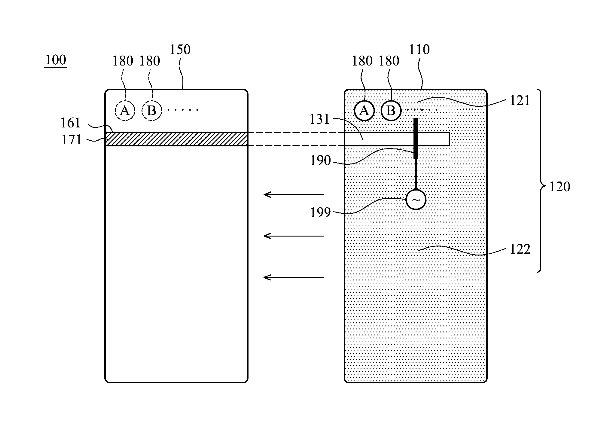
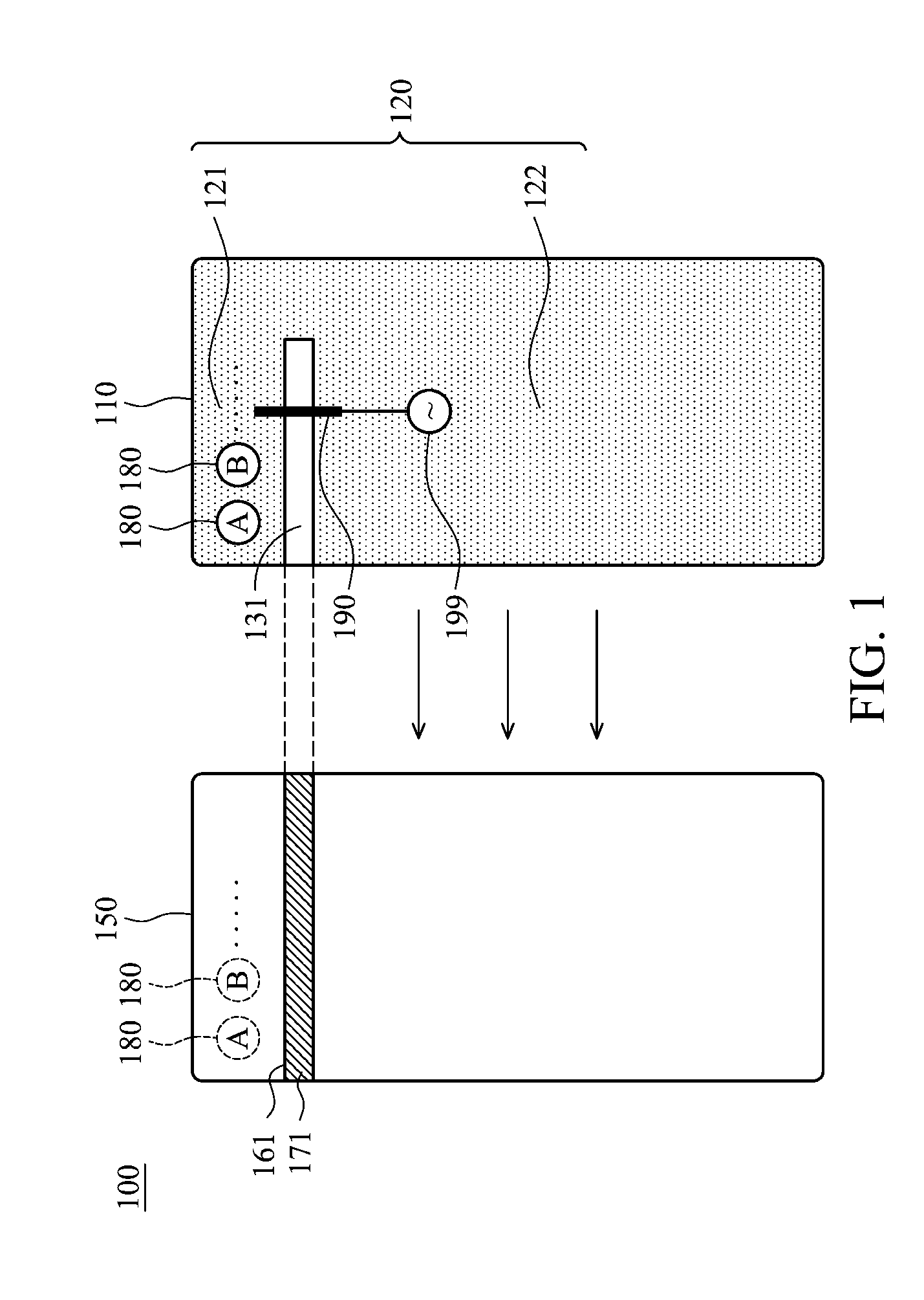
[0034]The subject application is mainly related to a metal housing (or a metal appearance element) and disposition of a PCB (Printed Circuit Board) with different shapes. An antenna structure can operate in the desired resonant band by appropriately adjusting the antenna feeding point, the feeding matching impedance, and the length and width of the slot on the PCB. In addition, the antenna structure is electrically coupled to the metal housing such that the metal housing is considered an extension of the antenna structure. Accordingly, the metal housing neither shields nor negatively affects the radiation of the antenna structure. The subject application further provides a mobile phone design integrated with a whole metal housing. The detailed descriptions and implements are illustrated as follows.

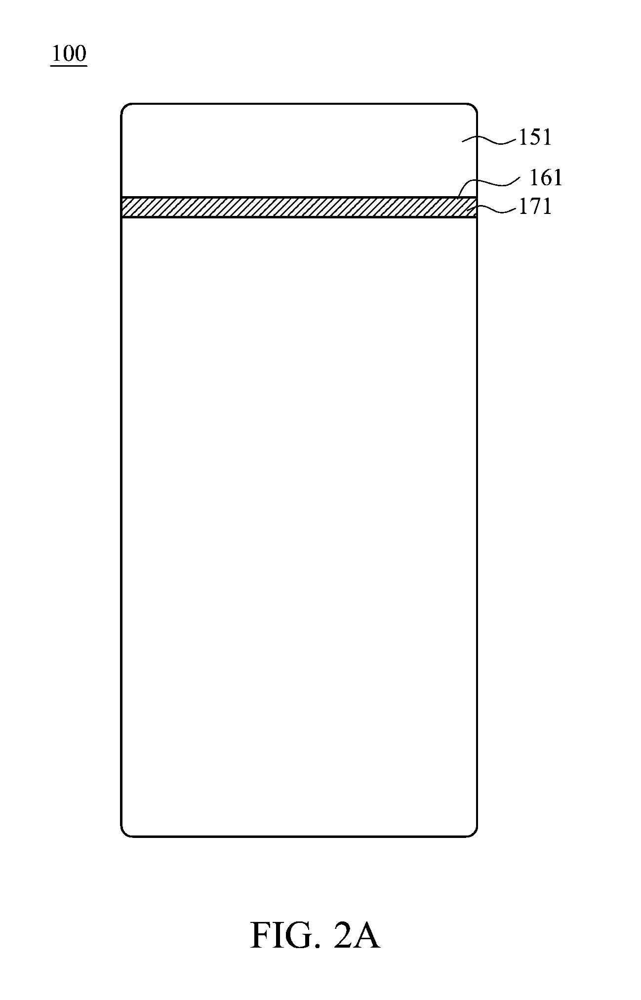
[0035]FIG. 1 is a diagram illustrating a mobile device 100 according to an embodiment of the invention. The mobile device 100 may be a cellular phone, a tablet computer, or a notebook comp...


PUM


Abstract

A mobile device includes a dielectric substrate, a metal layer, a metal housing, a nonconductive partition, at least one connection element, and a feeding element. The metal layer is disposed on the dielectric substrate, and includes an upper element and a main element, wherein a slot is formed between the upper element and the main element. The metal housing is substantially a hollow structure, and has a slit, wherein the slit is substantially aligned with the slot of the metal layer. The connection element couples the upper element of the metal layer to the metal housing. The feeding element is coupled to the upper element of the metal layer or coupled to the metal housing. An antenna structure is formed by the feeding element, the upper element of the metal layer, the connection element, and the metal housing.

Description

BACKGROUND OF THE INVENTION[0001]1. Field of the Invention[0002]The subject application generally relates to a mobile device and, more particularly, to a mobile device comprising an antenna structure with metal housing.[0003]2. Description of the Related Art[0004]With the progress of mobile communication technology, handheld devices like portable computers, mobile phones, multimedia players, and other hybrid functional portable electronic devices have become more common. To satisfy the user demand, handheld devices can usually perform wireless communication functions. Some devices cover a large wireless communication area, such as mobile phones using 2G, 3G, 4G and LTE (Long Term Evolution) systems and using frequency bands of 700 MHz, 800 MHz, 850 MHz, 900 MHz, 1800 MHz, 1900 MHz, 2100 MHz, 2300 MHz, 2500 MHz and 2600 MHz. Some devices cover a small wireless communication area, for example, mobile phones using Wi-Fi, Bluetooth, and WiMAX (Worldwide Interoperability for Microwave Ac...

Claims


Application Information

Patent Timeline
Patent Type & Authority Applications(United States)
IPC IPC(8): H01Q1/24H01Q13/10
CPCH01Q13/106H01Q1/243H01Q1/2266H01Q1/44H01Q1/50
Inventor TSAI, TIAO-HSINGCHIU, CHIEN-PINWU, HSIAO-WEIKUO, CHAO-CHIANG
Owner HTC CORP
Why Eureka
Try Eureka