Lamination layer type semiconductor package

a technology of semiconductor packages and layers, applied in semiconductor devices, semiconductor/solid-state device details, electrical devices, etc., can solve problems such as defects, and achieve the effect of minimizing warpage defects

Inactive Publication Date: 2014-05-29
SAMSUNG ELECTRO MECHANICS CO LTD
View PDF4 Cites 10 Cited by
  • Summary
  • Abstract
  • Description
  • Claims
  • Application Information

AI Technical Summary

Benefits of technology

[0014]An object of the present invention is to provide a lamination layer type semiconductor package capable of maintaining a thickness of a package on package structure at a minimum and minimizing warpage defect by mounting two chips so as to correspond to each other.

Problems solved by technology

However, the package on package structure according to the related art separately performs mold processes for molding chips and generates warpage at the upper package and the lower package at the time of mounting on a board of the mobile due to characteristic of a structure on which the upper package and the lower package are stacked, such that defect may be caused.

Method used


Image

  • Lamination layer type semiconductor package
  • Lamination layer type semiconductor package
  • Lamination layer type semiconductor package

Examples


Embodiment Construction

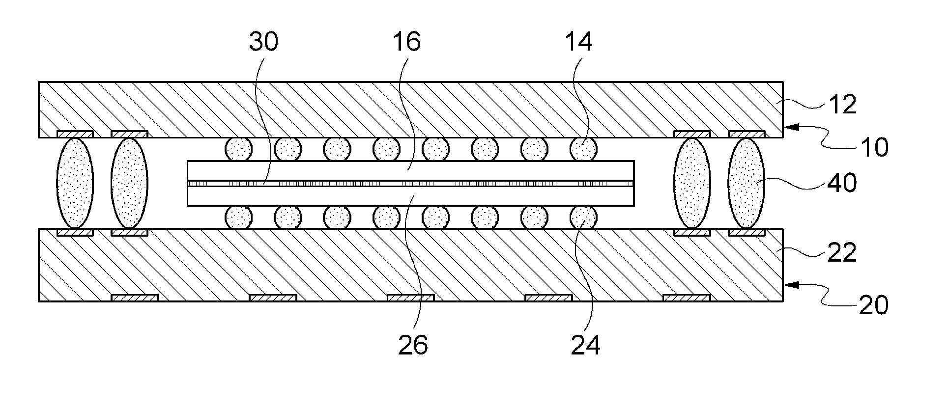
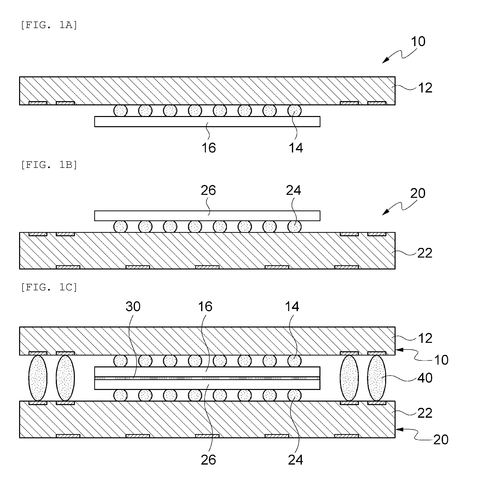
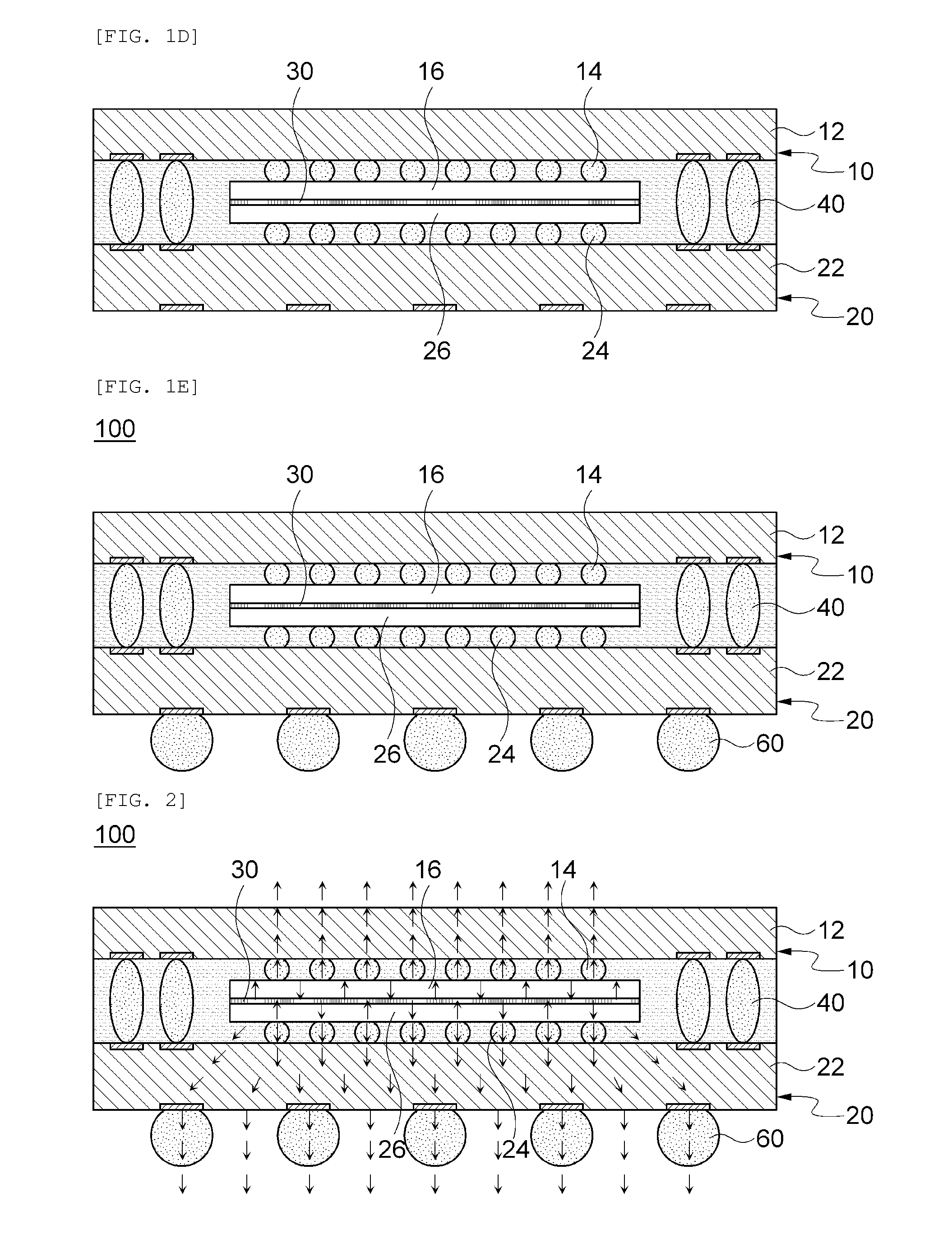
[0023]Hereinafter, a lamination layer type semiconductor package according to an exemplary embodiment of the present invention will be described in detail with reference to the accompanying drawings.

[0024]FIGS. 1A to 1E are illustration views showing processes of manufacturing a lamination layer type semiconductor package according to an exemplary embodiment of the present invention and FIG. 2 is an illustration view showing a process of dissipating heat of the lamination layer type semiconductor package according to the exemplary embodiment of the present invention.

[0025]As shown, the lamination layer type semiconductor package 100 according to the exemplary embodiment of the present invention includes an upper package 10 having an upper flip chip 16 mounted thereon, a lower package 20 having a lower flip chip 26 mounted thereon, a heat dissipation adhesive member 30 adhesively fixing the upper flip chip 16 and the lower flip chip 26 to each other, and a molding member 50 molding b...


PUM


Abstract

Disclosed herein is a lamination layer type semiconductor package, and more particularly, a lamination layer type semiconductor package capable of maintaining a thickness of a package on package structure at a minimum and minimizing a warpage defect by mounting two chips so as to correspond to each other. The lamination layer type semiconductor package includes: an upper package having an upper flip chip mounted on an upper substrate; a lower package having a lower flip chip mounted on a lower substrate and disposed so as to closely adhere the upper flip chip and the lower flip chip to each other; a heat dissipation adhesive member adhesively fixing the upper flip chip and the lower flip chip and dissipating heat generated from the upper flip chip and the lower flip chip; and a molding member molding between the upper substrate and the lower substrate.

Description

CROSS REFERENCE(S) TO RELATED APPLICATIONS[0001]This application claims the benefit under 35 U.S.C. Section 119 of Korean Patent Application Serial No. 10-2012-0134493, entitled “Lamination Layer Type Semiconductor Package” filed on Nov. 26, 2012, which is hereby incorporated by reference in its entirety into this application.BACKGROUND OF THE INVENTION[0002]1. Technical Field[0003]The present invention relates to a lamination layer type semiconductor package, and more particularly, to a lamination layer type semiconductor package capable of maintaining a thickness of a package on package structure at a minimum and minimizing a warpage defect by mounting two chips so as to correspond to each other.[0004]2. Description of the Related Art[0005]In general, a demand for portable information communication devices has recently increased in a market of electronic products. Therefore, various semiconductors and electric and electronic parts embedded in those products also tend to be manufac...

Claims


Application Information

Patent Timeline
Patent Type & Authority Applications(United States)
IPC IPC(8): H01L23/373
CPCH01L23/373H01L2224/16225H01L2224/32145H01L2224/73253H01L23/3737H01L23/49816H01L23/49833H01L23/3128H01L25/105H01L2225/1023H01L2225/1058H01L2225/1094H01L2924/15331H01L23/12H01L23/36
Inventor LEE, KYUNG HOKWON, HYUN BOKWOO, SEUNG WANHWANG, YOUNG NAMHAM, SUK JINKIM, PO CHULEUN, SO HYANGPARK, SE JUN
Owner SAMSUNG ELECTRO MECHANICS CO LTD
Why Eureka
Try Eureka