Image sensor and manufacturing method of image sensor

a manufacturing method and sensor technology, applied in the field of image sensor manufacturing method, can solve the problems of degrading image quality, uneven sensitivity, degrading image quality, etc., and achieve the effect of avoiding flares and less uneven sensitivity

Active Publication Date: 2006-07-18
COLLABO INNOVATIONS INC
View PDF7 Cites 11 Cited by
  • Summary
  • Abstract
  • Description
  • Claims
  • Application Information

AI Technical Summary

Benefits of technology

[0010]An object of the present invention, in view of the above problem, is to provide an image sensor of low shading and a manufacturing method of the image sensor, the image sensor having less uneven sensitivity and including an antireflective film for avoiding flares.
[0012]According to the image sensor manufactured by such processes as described above, it is possible to pattern each of the lightproof film over the wiring area and the transparent film over the imaging area. Thus, it is possible to make the height even between the top surface of the transparent film and that of the antireflective film. Consequently, it possible to manufacture the image sensor of low shading which has less uneven sensitivity than the conventional image sensor although it includes the antireflective film (lightproof film) for avoiding flares.
[0016]According to this structure, the lightproof film is formed either on or under the flat film. In both cases, the lightproof film does not exist sin the flat film, and thereby it is possible to maintain the thickness of the flat film on which the micro lenses are formed even between the central part and the ambient part of the imaging area. In the case that the lightproof film is formed on the flat film, the lightproof film is formed after the flat film. In the case that the lightproof film is formed under the flat film, the lightproof film is formed over the wiring area; the top surface of the lightproof film and that of the imaging area are made even; and the flat film on which the micro lenses are formed is formed over the lightproof film and the imaging area. Consequently, in both cases the lightproof film does not exist in the flat film, and thereby it is possible to maintain the thickness of the flat film on which the micro lenses are formed even between the central part and the ambient part of the imaging area. Thus, it is possible to manufacture the image sensor of low shading and the manufacturing method of the image sensor, the image sensor having less uneven sensitivity while including the antireflective film for avoiding flares.
[0020]According to the image sensor and its manufacturing method of the present invention, it is possible to manufacture the image sensor of low shading and the manufacturing method of the image sensor, the image sensor having less uneven sensitivity while including the antireflective film for avoiding flares. Also, one mask pattern can be used for the patterning of both the lightproof film and the transparent film.

Problems solved by technology

However, the problem with the conventional technology is that a step height is generated between the imaging area 2 and the area above the wiring area 3 including the antireflective film 4 for avoiding a flare, especially around the imaging area, thus causing an uneven sensitivity (shading), and thereby degrading image quality.
Consequently, an uneven sensitivity (shading) is created, thereby degrading image quality.

Method used


Image

  • Image sensor and manufacturing method of image sensor
  • Image sensor and manufacturing method of image sensor
  • Image sensor and manufacturing method of image sensor

Examples


second embodiment

(Second Embodiment)

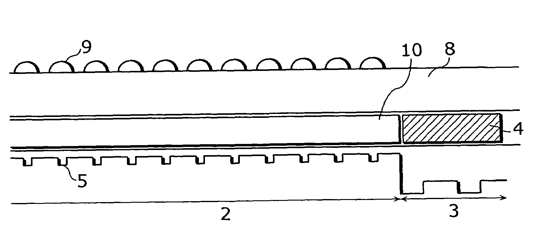
[0062]FIG. 4A–FIG. 4C show section views of the image sensor according to the second embodiment in the order of the manufacturing processes. While the transparent film 10 is formed after the formation of the lightproof film 4 according to the manufacturing method in FIG. 3, the lightproof film 4 is formed after the formation of the transparent film 10 in FIG. 4.

[0063]The manufacturing processes according to the second embodiment will be explained in the order of (101a)–(106a) as follows. However, the same processes as the first embodiment will be omitted, and the different processes will be mainly explained.

[0064](101a) The wiring area 3 is flattened in the same manner as (101).

[0065](102a) The transparent film 10 is formed on the imaging area 2 in the same manner as (104). FIG. 4A is a section view of this formation.

[0066](103a) The colorable photoresist of the same thickness (0.3–0.9 μm) as the transparent film is formed on the wiring area in the same manner as ...

third embodiment

(Third Embodiment)

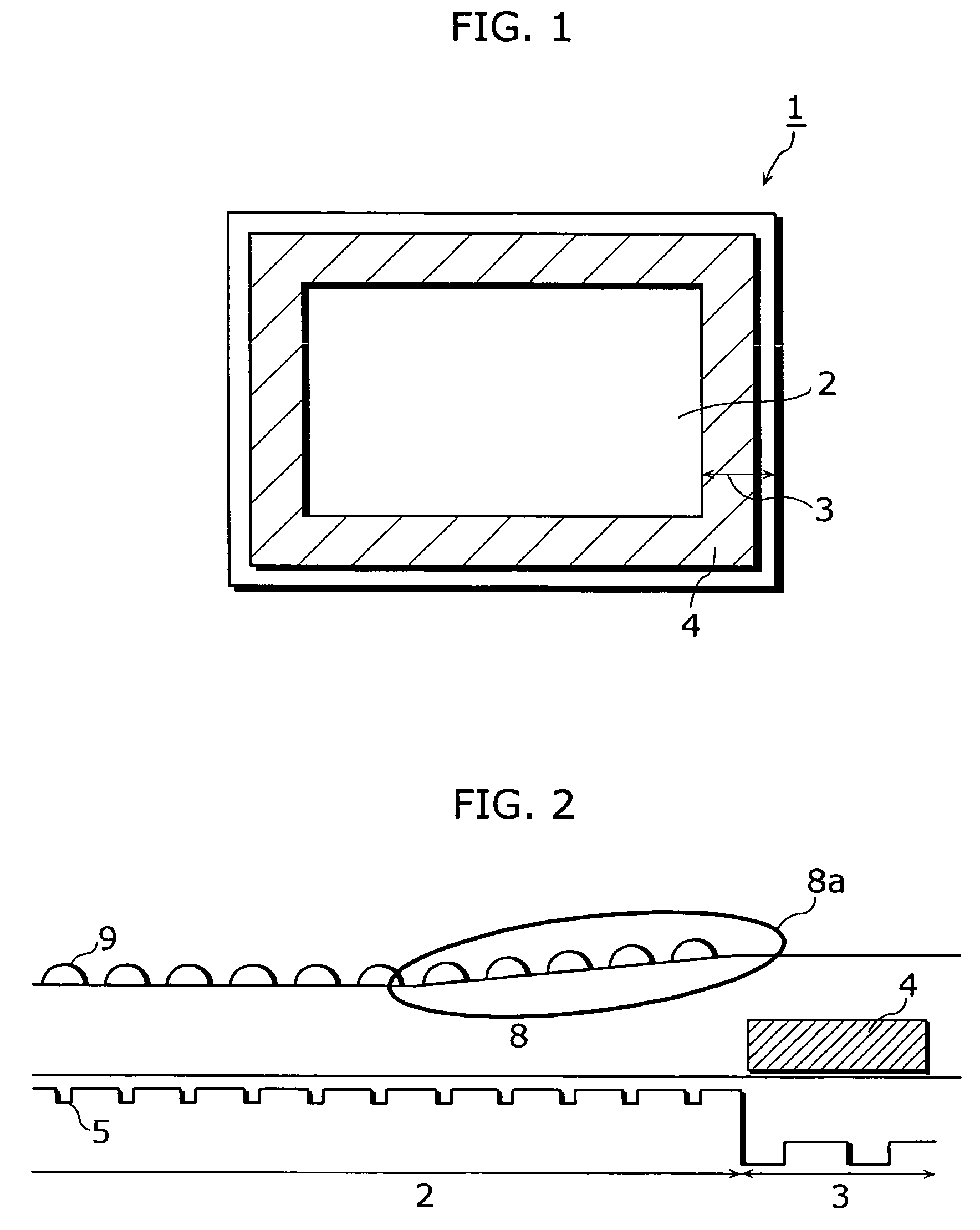
[0072]FIG. 5A–FIG. 5B show section views of the image sensor according to the third embodiment in the order of the manufacturing processes. The manufacturing processes according to the third embodiment will be explained in the order of (901)–(905) as follows.

[0073](901) The wiring area 3 is flattened in the same manner as (101).

[0074](902) The flat film (the transparent film 8) for forming micro lenses on top is applied (0.3–5.0 μm).

[0075](903) The micro lenses 9 are formed. FIG. 5A is a section view of this formation.

[0076](904) Over the wiring area 3, the colorable photoresist is formed by applying it (0.3–0.9 μm), exposing it to light, and developing it. The photoresist can be either of a negative type or a positive type.

[0077](905) The colorable photoresist is colored black (Black). Thus, the lightproof film 4 is formed. FIG. 5B shows the section view of this formation.

[0078]In this manner, the lightproof film 4 is formed on the flat film (the transparent film ...

fourth embodiment

(Fourth Embodiment)

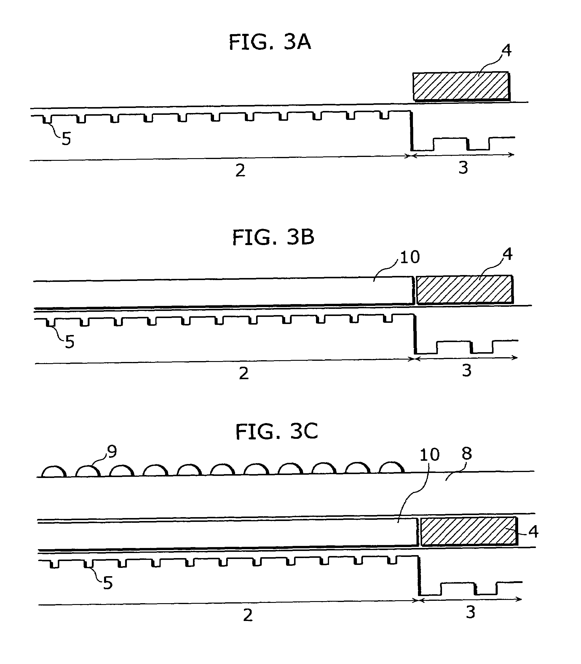
[0109]FIG. 7A–FIG. 7B show the section views of the image sensor according to the fourth embodiment in the order of the manufacturing processes. The manufacturing processes of the present embodiment will be explained in the order of (501)–(505).

[0110](501) On the wiring area 3, the colorable photoresist is formed by applying it (0.3–0.9 μm), exposing it to light, and developing it so as to flatten the top surface of the wiring area 3. The photoresist can be either of a negative type or a positive type.

[0111](502) The colorable photoresist is colored black (Black). Thus, the lightproof film 4 is formed. FIG. 7A shows the section view of this formation.

[0112](503) On Black and the imaging area 2, the flat film (the transparent film 8) for forming micro lenses on top is formed (0.3–5.0 μm).

[0113](504) The micro lenses are formed. FIG. 7B shows the section view of this formation.

[0114]As described above, according to the image sensor of the fourth embodiment, i) the l...


PUM


Abstract

In a manufacturing method of an image sensor, a lightproof film (an antireflective film for avoiding flares) is formed over a wiring area; a transparent film is formed over an imaging area using a material capable of patterning; a transparent film, for forming micro lense on top, is formed on the transparent film, wherein a height of the top surfaces of the transparent film and the lightproof film are evenly formed.

Description

BACKGROUND OF THE INVENTION[0001](1) Field of the Invention[0002]The present invention relates to a manufacturing method of an image sensor comprising an imaging area which includes a plurality of pixel units and a wiring area around the imaging area, and in particular, to the improvement of a shading characteristic.[0003](2) Description of the Related Art[0004]Recently, the sensitivity of an image sensor has been improved by forming a micro lens on each pixel and collecting an incident light on each of a plurality of pixel units.[0005]FIG. 1 is a top view of such an image sensor as described above. In FIG. 1, the image sensor comprises an imaging area 2 including a plurality of pixel units (a photodiode), a wiring area 3 around the imaging area 2, and an antireflective film 4. The antireflective film 4 is a lightproof filter of low transmittance (e.g. black), formed on the wiring area 3 surrounding the imaging area 2, and is equipped so as to prevent flares caused by a reflected in...

Claims


Application Information

Patent Timeline
Patent Type & Authority Patents(United States)
IPC IPC(8): H01L21/00H01L27/14H01L27/146H01L31/0216H04N5/335H04N5/369
CPCH01L27/14603H01L31/02164H01L27/14627H01L27/1462
Inventor SAKOH, HIRSOSHIOKAMOTO, HIROSHINAGAYOSHI, RYOICHI
Owner COLLABO INNOVATIONS INC
Why Eureka
Try Eureka