Displacement sensor with segmented ring microresonator

a microresonator and displacement sensor technology, applied in the field of waveguide microresonators, can solve the problems of limiting the sensitivity of the sensor, affecting the effect of the nanobeam on the resonance wavelength, and undergoing optical losses in the analysis beam transiting in the microresonator

Active Publication Date: 2020-03-03
COMMISSARIAT A LENERGIE ATOMIQUE ET AUX ENERGIES ALTERNATIVES
View PDF8 Cites 1 Cited by
  • Summary
  • Abstract
  • Description
  • Claims
  • Application Information

AI Technical Summary

Benefits of technology

[0025]When the ancillary moveable element is located between two elementary waveguides, it cuts the optical path of the light beam propagating in the microresonator, which results in a considerable increase in the losses at the resonance wavelengths of the microresonator and / or a considerable modification of the phase in the microresonator.
[0034]The sensitivity of detection, or even of measurement, of the mechanical deformation of the microresonator is thereby increased.
[0035]Since the microresonator is constituted of distinct elementary waveguides, it is possible to free the movement of some of them, relative to the others.
[0036]Mechanical stresses, which in the prior art were not capable of deforming the microresonator, can then lead to the displacement of one or more elementary waveguides relative to the others. This displacement results in a variation in a signal having transited via the microresonator. The sensitivity of the microresonator to external mechanical stresses is thereby increased.
[0042]The optical sensor according to the invention offers increased sensitivity to the measurement of nanometric displacements.

Problems solved by technology

The part of the analysis beam transiting in the microresonator undergoes optical losses therein, due notably to absorption by the surrounding medium.
The influence of the nanobeam on the resonance wavelengths remains however quite restricted, which limits the sensitivity of the sensor.

Method used


Image

  • Displacement sensor with segmented ring microresonator
  • Displacement sensor with segmented ring microresonator
  • Displacement sensor with segmented ring microresonator

Examples


first embodiment

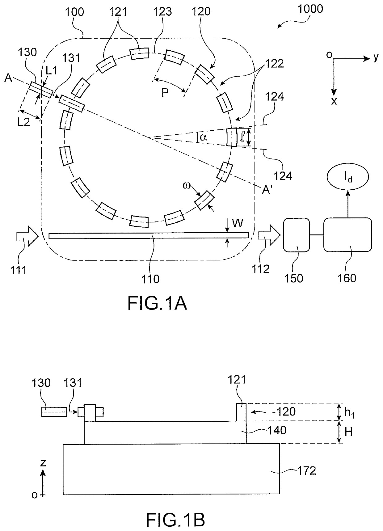
[0045]FIGS. 1A and 1B illustrate in a schematic manner an optical sensor according to the invention, respectively in a top view and in a sectional view;

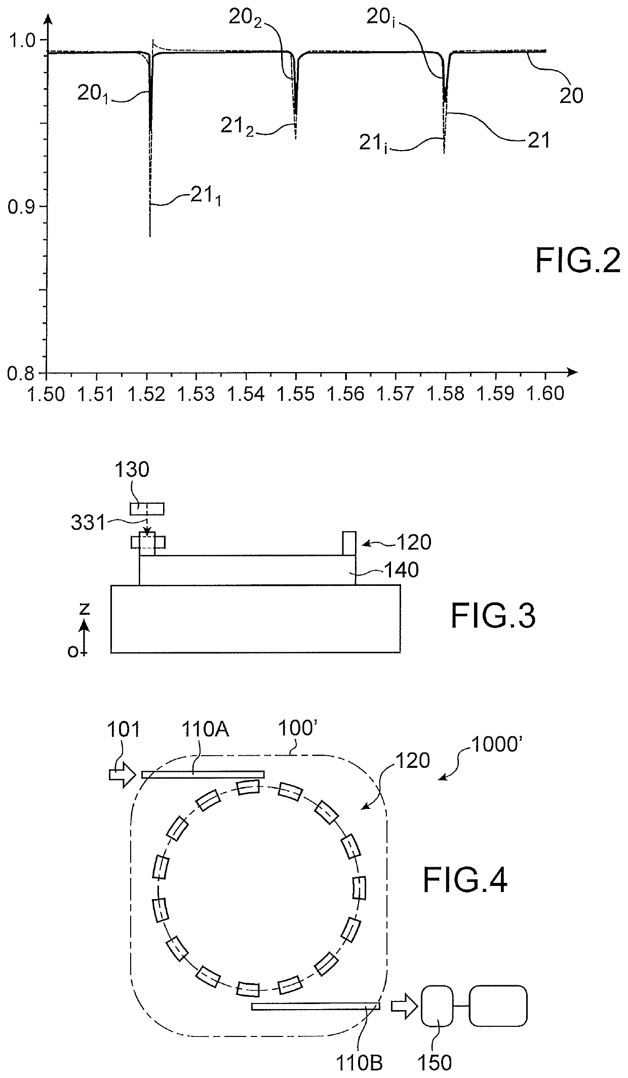
[0046]FIG. 2 illustrates transmission spectra obtained by means of the sensor of FIGS. 1A and 1B;

[0047]FIG. 3 illustrates in a schematic manner a first alternative of the embodiment of FIGS. 1A and 1B;

[0048]FIG. 4 illustrates in a schematic manner a second alternative of the embodiment of FIGS. 1A and 1B;

second embodiment

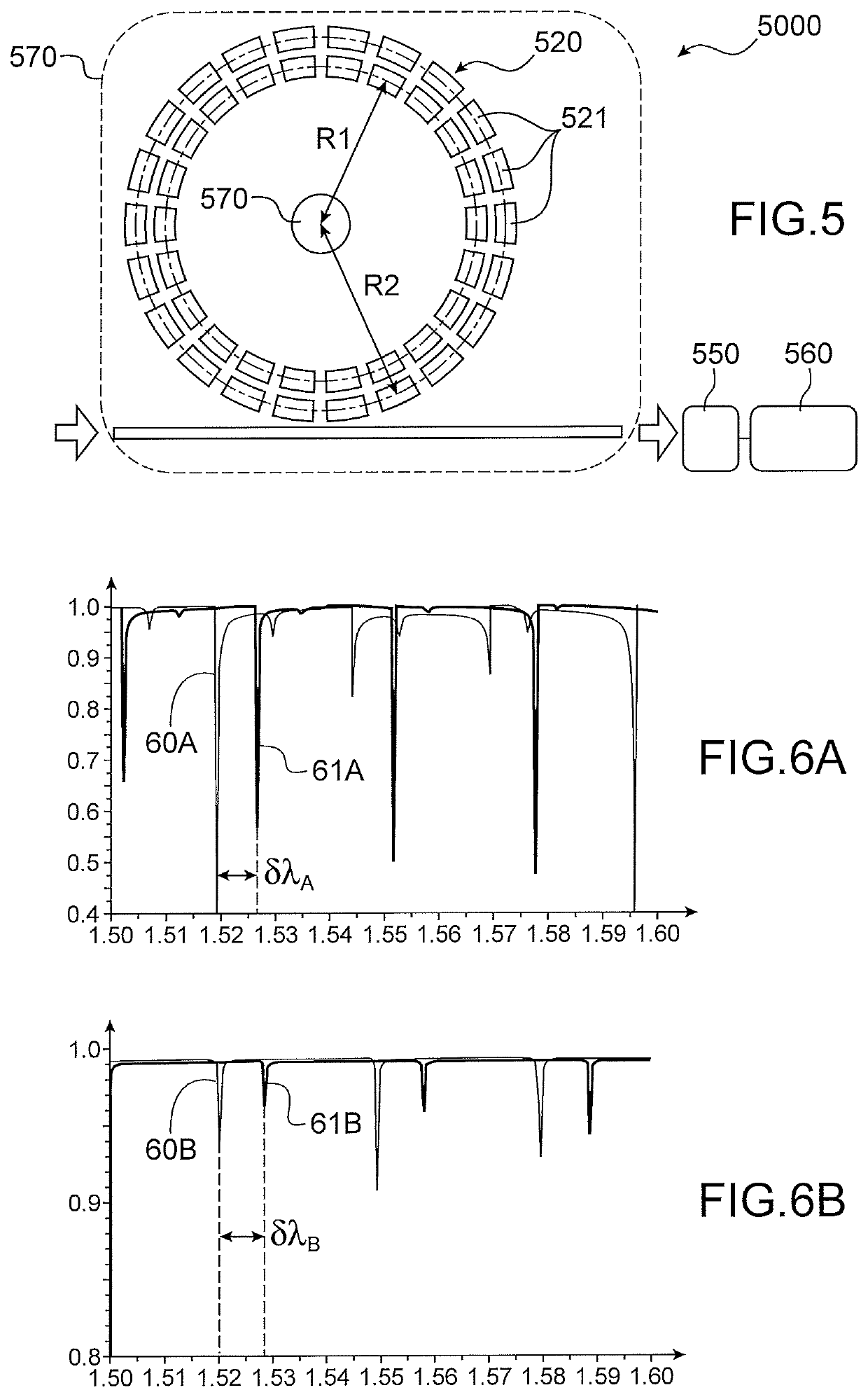
[0049]FIG. 5 illustrates in a schematic manner an optical sensor according to the invention;

[0050]FIGS. 6A and 6B illustrate a comparison of the transmission spectrum variation obtained by means of a sensor according to the prior art, and by means of a sensor according to the invention;

[0051]FIGS. 7A and 7B illustrate in a schematic manner a first alternative of suspended layout of the microresonator according to the invention;

[0052]FIGS. 8A and 8B illustrate in a schematic manner a second alternative of suspended layout of the microresonator according to the invention;

third embodiment

[0053]FIGS. 9A to 9D illustrate different alternatives of the microresonator of an optical sensor according to the invention;

[0054]FIGS. 10A and 10B illustrate two alternatives of a coupling zone of an injection and extraction waveguide according to the invention; and

[0055]FIG. 11 illustrates in a schematic manner a method for manufacturing an optical device according to the invention.


PUM

PropertyMeasurementUnit
wavelengthaaaaaaaaaa
distanceaaaaaaaaaa

Abstract

An optical sensor includes an optical device including a microresonator, laid out to guide a light beam along a closed loop optical path, and an injection and / or extraction waveguide, optically coupled to the microresonator; a photodetector, arranged at the output of the injection and / or extraction waveguide; and an analysis device, receiving a signal supplied by the photodetector, and deducing therefrom information relative to a displacement. The microresonator is constituted of a plurality of elementary waveguides spaced apart from each other, and arranged one after the other according to a loop shaped layout. The optical sensor offers increased sensitivity to the measurement of nanometric displacements.

Description

TECHNICAL FIELD[0001]The invention relates to the field of waveguide microresonators, and their use for detecting, or even measuring, a deformation of the microresonator or a displacement in the near field of said microresonator.PRIOR ART[0002]The article “Optical racetrack resonator transduction of nanomechanical cantilevers”, by V. T. K. Sauer & al., Nanotechnology, vol. 25 (2014), describes the measurement of the displacement of a nanobeam, near to a waveguide microresonator.[0003]The waveguide microresonator is constituted of a ring shaped curved waveguide, called ring microresonator.[0004]The ring microresonator does not comprise cladding. It is the surrounding medium that acts as cladding.[0005]This microresonator is coupled to an injection and extraction waveguide, by evanescent coupling.[0006]Evanescent coupling corresponds to an interaction between a guided mode of the injection and extraction waveguide, and a guided mode of the microresonator, which results in a transfer o...

Claims


Application Information

Patent Timeline
Patent Type & Authority Patents(United States)
IPC IPC(8): G01C19/72G02B6/293
CPCG01C19/727G02B6/29338G01D5/35338G02B6/29341
Inventor TAUREL, BORISBOUTAMI, SALIMDURAFFOURG, LAURENT
Owner COMMISSARIAT A LENERGIE ATOMIQUE ET AUX ENERGIES ALTERNATIVES
Why Eureka
Try Eureka