Image sensor and manufacturing method of image sensor
a manufacturing method and image sensor technology, applied in the field of image sensor manufacturing method, can solve the problems of degrading image quality, degrading image quality, and photodiode not acquiring enough incident ligh
- Summary
- Abstract
- Description
- Claims
- Application Information
AI Technical Summary
Benefits of technology
Problems solved by technology
Method used
Image
Examples
first embodiment
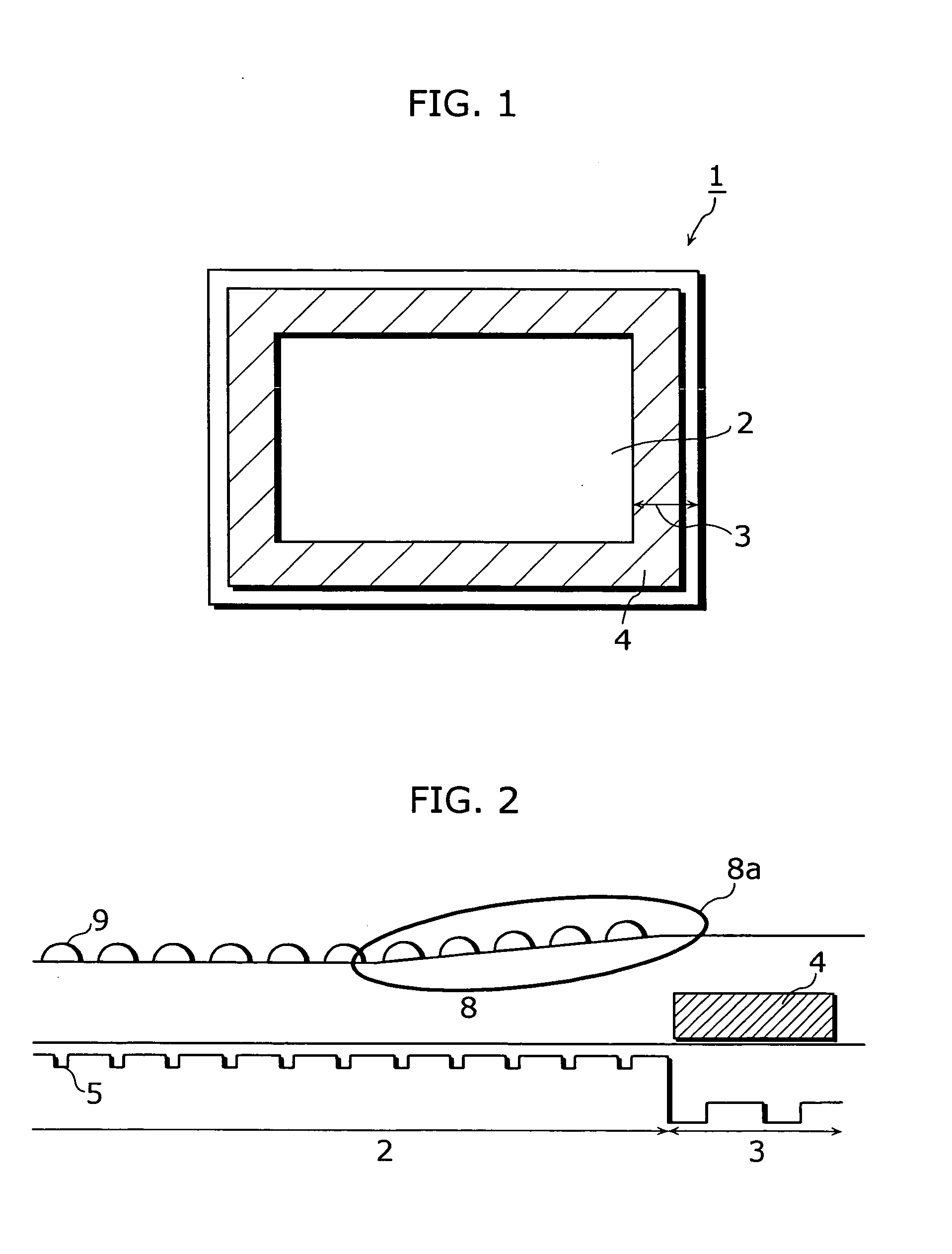
[0028] A sketchy top view of the image sensor according to the first embodiment is the same as FIG. 1, and comprises an imaging area2 including a plurality of pixel units (photodiode5), a wiring area3, and a lightproof film4 on the wiring area3.
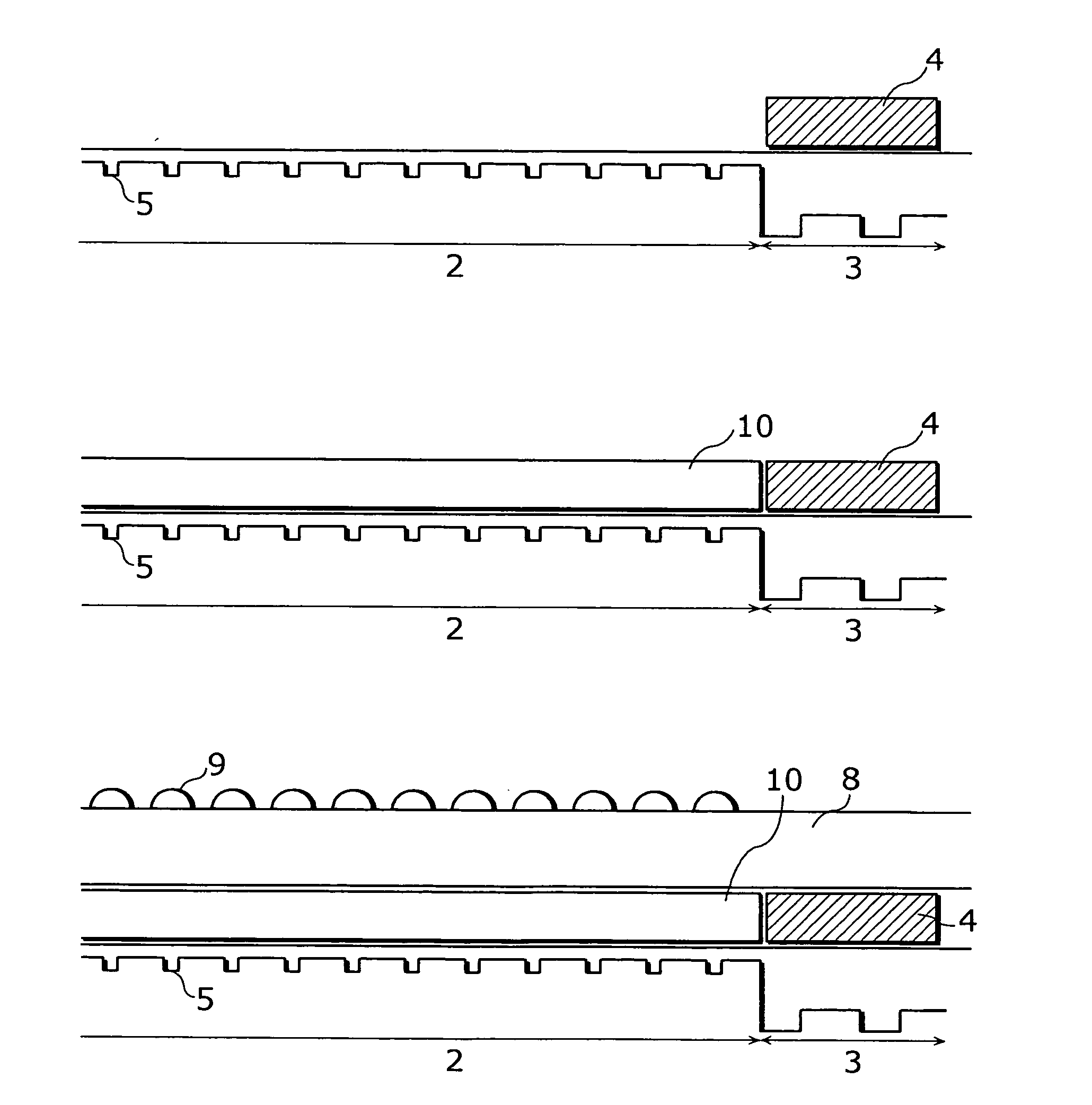
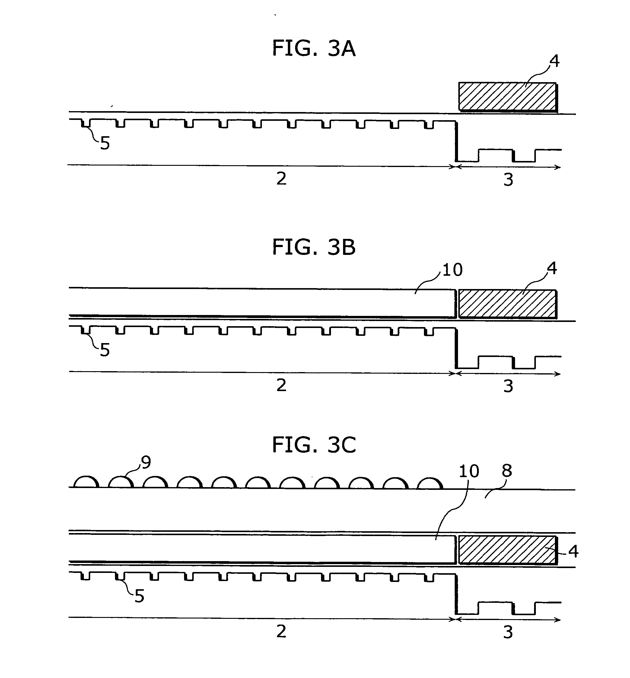
[0029] In the manufacturing method of the image sensor according to the first embodiment, a transparent film10 is formed on the imaging area2 using a material capable of patterning and of the same thickness as an anti-flare pattern, either before or after the anti-flare pattern of low transmittance (lightproof film4) is formed on the wiring area3. In the formations of the transparent film10 and the lightproof film4, the height is made even between the top surface of the transparent film10 and that of the lightproof film4. The micro lenses are formed after a transparent film such as acryl is applied. Consequently, a step height caused by the anti-flare pattern (lightproof film4) is eliminated, thus the image sensor of low shading can be manufa...
second embodiment
[0062] FIG. 4A-FIG. 4C show section views of the image sensor according to the second embodiment in the order of the manufacturing processes. While the transparent film10 is formed after the formation of the lightproof film4 according to the manufacturing method in FIG. 3, the lightproof film4 is formed after the formation of the transparent film10 in FIG. 4.
[0063] The manufacturing processes according to the second embodiment will be explained in the order of (110a)-(106a) as following. However, the same processes as the first embodiment will be omitted, and the different processes will be mainly explained.
[0064] (101a) The wiring area3 is flattened in the same manner as (101).
[0065] (102a) The transparent film10 is formed on the imaging area2 in the same manner as (104). FIG. 4A is a section view of this formation.
[0066] (103a) The colorable photoresist of the same thickness (0.3-0.9 .mu.m) as the transparent film is formed on the wiring area in the same manner as (102).
[0067] (10...
third embodiment
[0072] FIG. 5A-FIG. 5B show section views of the image sensor according to the third embodiment in the order of the manufacturing processes. The manufacturing processes according to the third embodiment will be explained in the order of (901)-(905) as following.
[0073] (901) The wiring area3 is flattened in the same manner as (101).
[0074] (902) The flat film(the transparent film8) for forming micro lenses on top is applied (0.3-5.0 .mu.m).
[0075] (903) The micro lenses9 are formed. FIG. 5A is a section view of this formation.
[0076] (904) Over the wiring area3, the colorable photoresist is formed by applying it (0.3-0.9 .mu.m), exposing it to light, and developing it. The photoresist can be either of a negative type or a positive type.
[0077] (905) The colorable photoresist is colored black (Black). Thus, the lightproof film4 is formed. FIG. 5B shows the section view of this formation.
[0078] In this manner, the lightproof film4 is formed on the flat film (the transparent film8) for form...
PUM
 Abstract
Description
Claims
Application Information


