Display device and driving method of display device

a display device and driving method technology, applied in static indicating devices, instruments, electroluminescent light sources, etc., can solve the problems of difficult to realize high definition and multiple gray scales, area gray scale methods, etc., to improve display quality, reduce pseudo contours, and improve duty ratio

Active Publication Date: 2014-06-05
SEMICON ENERGY LAB CO LTD
View PDF21 Cites 6 Cited by
  • Summary
  • Abstract
  • Description
  • Claims
  • Application Information

AI Technical Summary

Benefits of technology

[0014]In view of such problems, it is an object of the present invention to provide a display device composed of few sub-frames and that can reduce a pseudo contour, where multiple gray scales are possible as well, and a driving method using the display device.
[0019]Note that, as for a switch shown in the present invention, switches of various modes can be used. As an example, there is an electrical switch, a mechanical switch, or the like. In other words, the switches are not particularly limited as long as current flow can be controlled and various switches can be used. For example, the switches may be a transistor, a diode (a PN diode, a PIN diode, a Schottky diode, a transistor connected as a diode, or the like) or a logic circuit that is a combination thereof. Thus, in a case of using a transistor as the switch, the transistor operates as a mere switch; therefore, the polarity (conductivity type) of the transistor is not particularly limited. However, in a case where lower off-current is desired, it is desirable to use a transistor having a polarity with lower off-current. As the transistor with low off-current, a transistor provided with an LDD region, a transistor having a multi-gate structure, or the like can be used. In addition, it is desirable to use an N-channel transistor when a transistor to be operated as a switch operates in a state where potential of a source terminal thereof is close to a lower potential side power supply (such as Vss, GND, or 0 V), whereas it is desirable to use a P-channel transistor when a transistor operates in a state where potential of a source terminal thereof is close to a higher potential side power supply (such as Vdd). This is because the absolute value of a gate-source voltage can be increased, and the transistor easily operates as a switch. Note that the switch may be of a CMOS type using both the N-channel transistor and the P-channel transistor. When the CMOS-type switch is employed, voltage outputted through the switch (that is, voltage inputted into the switch) may be high or low with respect to the outputted voltage and the switch can be operated appropriately even when the situation is changed.
[0034]Note that, according to the present invention, one pixel shows one color element. Therefore, in a case of a color display device including color elements of R (red), G (green), and B (blue), a minimum unit of an image includes three pixels of R, G, and B. Note that the color element is not limited to three colors and three or more colors may be used, or a color other than RGB may also be used. For example, RGBW may be employed by adding white (W). In addition, RGB may be added with one or more of yellow, cyan, magenta, and the like, for example. Moreover, for example, as for at least one color of RGB, a similar color may be added. For example, R, G, B1, and B2 may be used. Both B1 and B2 are blue but have a different wavelength. By using such a color element, it is possible to perform display that is much similar to the real and to reduce power consumption.
[0037]According to the present invention, it is possible to reduce a pseudo contour and to perform multiple gray scales as well by combining an area gray scale method and a time gray scale method. Therefore, it becomes possible to improve display quality and to view a clear image. In addition, it is possible to improve a duty ratio (a ratio of a lighting period per one frame), and voltage applied to a light-emitting element is reduced. Thus, power consumption can be reduced, and deterioration of the light-emitting element can be suppressed.

Problems solved by technology

The number of the sub-pixels cannot be increased; therefore, it is difficult to realize high definition and multiple gray scales.
This can be given as a disadvantage of the area gray scale method.
Although various methods for reducing pseudo contour have been conventionally suggested, a sufficient effect for reducing pseudo contour has not been obtained yet and further improvement has been urged.

Method used


Image

  • Display device and driving method of display device
  • Display device and driving method of display device
  • Display device and driving method of display device

Examples


embodiment mode 1

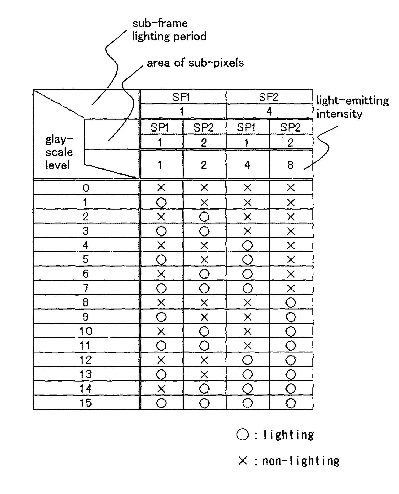
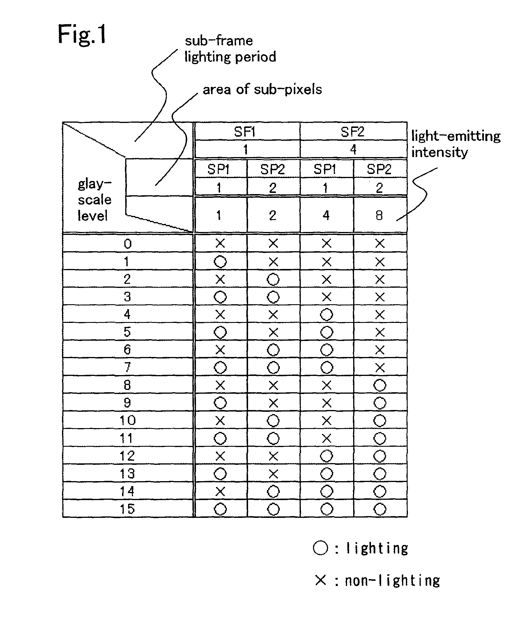
[0111]This embodiment mode will explain an example of applying a driving method of the present invention to a case of 4-bit display (16 gray scales) and a case of 6-bit display (64 gray scales).

[0112]The driving method of this embodiment mode is combined with an area gray scale method by which gray scale display is performed by dividing one pixel into a plurality of sub-pixels and controlling the number or area of lighting sub-pixels and a time gray scale method by which gray scale display is performed by dividing one frame into a plurality of sub-frames, each of which is weighted with respect to the number of light emissions and a light-emitting period, and then the total weight is differentiated for each gray scale. In other words, one pixel is divided into m (m is an integer number of m≧2) of sub-pixels to have an area ratio of the m sub-pixels 20:21:22: . . . :2m-3:2m-2:2m-1. In addition, one frame is divided into n (n is an integer number of n≧2) of sub-frames to have a ratio i...

embodiment mode 2

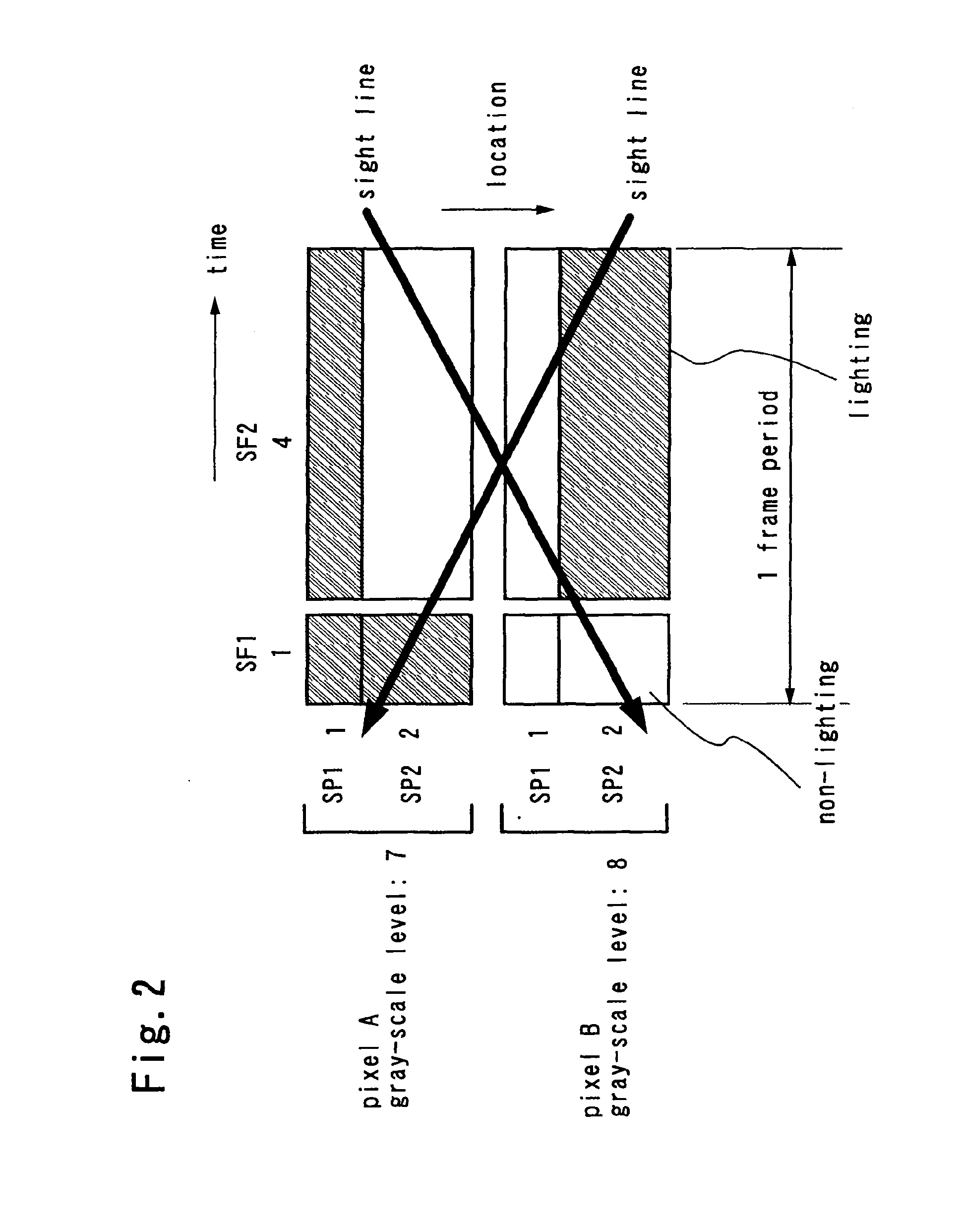
[0176]This embodiment mode will describe an example of a timing chart. This embodiment mode will be explained by giving, as an example, a case (FIG. 7) where one pixel is divided into two sub-pixels (SP1 and SP2) so that an area ratio of each sub-pixel becomes 1:2 and one frame is divided into three sub-frames (SF1, SF2, and SF3) so that a ratio of a lighting period in each sub-frame becomes 1:4:16.

[0177]Here, the sub-pixels respectively have the following area: SP1=1 and SP2=2, and the sub-frames respectively have the following lighting periods: SF1=1, SF2=4, and SF3=16.

[0178]First, FIG. 24 shows a timing chart in the case where a period where a signal is written to a pixel and a lighting period where are separated.

[0179]Note that a timing chart is a diagram showing light emission of a pixel in one frame, and a horizontal indicates a time whereas a vertical direction indicates a row where pixels are arranged.

[0180]First, signals for one screen are inputted to all pixels in a signal...

embodiment mode 3

[0250]This embodiment mode will describe a layout of a pixel in a display device according to the present invention. As an example, FIG. 35 shows a layout diagram of the circuit diagram shown in FIG. 25. Note that the circuit diagram and the layout diagram are not limited to FIG. 25 and FIG. 35.

[0251]First and second select transistors 3511 and 3521, first and second driving transistors 3513 and 3523, first and second holding capacitors 3512 and 3522, electrodes 3514 and 3524 of first and second light-emitting elements, a signal line 3515, a power supply line 3516, and first and second scanning lines 3517 and 3527 are arranged in FIG. 35. As for a sub-pixel 1 (SP1), a source electrode and a drain electrode of the first select transistor 3511 are each connected to the signal line 3515 and a gate electrode of the first driving transistor 3513. A gate electrode of the first select transistor 3511 is connected to the first scanning line 3517. A source electrode and a drain electrode of ...


PUM


Abstract

It is an object of the present invention to reduce a cause of pseudo contour when display is performed with a time gray scale method. According to the present invention, one pixel is divided into m sub-pixels so that an area ratio of each sub-pixel becomes 20:21:22: . . . :2m-3:2m-2:2m-1 (m is an integer number of m≧2), and one frame is divided into n sub-frames so that a ratio of a lighting period in each sub-frame becomes 20: 2m:22m: . . . :2(n-3)m:2(n-2)m:2(n-1)m (n is an integer number of n≧2). Then, a gray scale is expressed by controlling a manner of lighting in each of the m sub-pixels in each of the n sub-frames.

Description

CROSS-REFERENCE TO RELATED APPLICATIONS[0001]This application is a divisional of U.S. application Ser. No. 11 / 427,427, filed Jun. 29, 2006, now pending, which claims the benefit of a foreign priority application filed in Japan as Serial No. 2005-194699 on Jul. 4, 2005, both of which are incorporated by reference.BACKGROUND OF THE INVENTION[0002]1. Field of the Invention[0003]The present invention relates to a display device and a driving method thereof. In particular, the present invention relates to a display device to which an area gray scale method is applied and a driving method thereof.[0004]2. Description of the Related Art[0005]In recent years, a so-called self-luminous type display device having a pixel that is formed of a light-emitting element such as a light-emitting diode (LED) has been attracting attention. As a light-emitting element used for such a self-luminous type display device, an organic light-emitting diode (OLED) (also called an organic EL element, an electro ...

Claims


Application Information

Patent Timeline
Patent Type & Authority Applications(United States)
IPC IPC(8): G09G3/20H05B44/00
CPCG09G3/2029G09G3/2033G09G3/2074G09G3/2077G09G3/3233G09G2300/0426G09G2300/0452G09G2300/0814G09G2300/0842G09G2310/0205G09G2310/0221G09G2310/0251G09G2310/0262G09G2320/0214G09G2320/0261G09G2320/0266G09G2320/0276H10K59/351H10K59/35G09G3/2003
Inventor SHISHIDO, HIDEAKIKIMURA, HAJIMEYAMAZAKI, SHUNPEI
Owner SEMICON ENERGY LAB CO LTD
Why Eureka
Try Eureka