Display device and driving method of display device

a display device and transistor technology, applied in static indicating devices, instruments, electroluminescent light sources, etc., can solve the problems of inability to accurately write video signals, inability to reduce the luminance of light-emitting elements, and inability to take up a lot of time, so as to improve image quality and reduce the effect of luminance variation

Inactive Publication Date: 2010-06-15
SEMICON ENERGY LAB CO LTD
View PDF16 Cites 18 Cited by
  • Summary
  • Abstract
  • Description
  • Claims
  • Application Information

AI Technical Summary

Benefits of technology

[0038]Note that, in the present invention, a transistor of various modes can be applied. Thus, a type of transistor that can be applied is not limited. Therefore, a thin film transistor (TFT) having a non-single crystalline semiconductor film typified by amorphous silicon or polycrystalline silicon, or the like can be applied. Accordingly, a display device can be manufactured even when a manufacturing temperature is not high or with a low cost, over a large-sized substrate or a transparent substrate, or by transmitting light through the transistor. In addition, a MOS transistor, which is formed using a semiconductor substrate or an SOI substrate, a junction transistor, a bipolar transistor, or the like can be applied. Accordingly, a transistor with less variation can be manufactured, a transistor having high current supply capacity can be manufactured, a transistor small in size can be manufactured, or a circuit with low power consumption can be formed. In addition, a transistor using a compound semiconductor such as ZnO, a-InGaZnO, SiGe, or GaAs, further a thin film transistor thinning the transistor or the like can be applied. Accordingly, a display device can be manufactured even when a manufacturing temperature is not high or at a room temperature, or by forming a transistor directly on a substrate having low heat resistance, for example, a plastic substrate or a film substrate. In addition, such a transistor that is manufactured using an ink-jet or a printing method can be applied. Accordingly, a display device can be manufactured at a room temperature, in a low degree of a vacuum, or with a large-sized substrate. Moreover, a display device can be manufactured without using a mask (a reticle); therefore, a layout of a transistor can be changed easily. Further, a transistor using an organic semiconductor or a carbon nanotube, or other transistors can be applied. Accordingly, a transistor can be formed over a flexible substrate. Note that hydrogen or halogen may also be contained in the non-single crystalline semiconductor film. In addition, various substrates can be used as a type of substrate where a transistor is disposed, and the substrate is not limited to a specific one. Thus, a transistor can be disposed over a single-crystalline substrate, an SOI substrate, a glass substrate, a quartz substrate, a plastic substrate, a paper substrate, a cellophane substrate, a stone material substrate, a stainless steel substrate, a substrate having stainless steel foil, or the like, for example. Furthermore, a transistor may also be formed over one substrate and thereafter the transistor is moved to another substrate to be disposed over another substrate. By using these substrates, a transistor having a preferable characteristic can be formed, a transistor with low power consumption can be formed, a device unlikely to break can be obtained, or heat resistance can be given to a transistor.
[0039]Note that, as for the switches described in the present invention, one in various modes can be used, and there are, for example, an electrical switch, a mechanical switch, and the like. In other words, the switches are not particularly limited as long as current flow can be controlled and various switches can be used. For example, the switches may be a transistor, a diode (for example, a PN diode, a PIN diode, a Schottky diode, a transistor connected as a diode, or the like), a thyristor, or a logic circuit that is a combination thereof. Thus, in a case of using a transistor as the switch, the transistor operates as a mere switch; therefore, the polarity (conductivity type) of the transistor is not particularly limited. However, in a case where lower off-current is desired, it is desirable to use a transistor having a polarity with lower off-current. As the transistor with low off-current, a transistor provided with an LDD region, a transistor having a multi-gate structure, or the like can be used. In addition, it is desirable to use an N-channel transistor when a transistor to be operated as a switch operates in a state where potential of a source terminal thereof is close to a lower potential side power supply (such as VSS, GND, or 0 V), whereas it is desirable to use a P-channel transistor when a transistor operates in a state where potential of a source terminal thereof is close to a higher potential side power supply (such as VDD). This is because the absolute value of a gate-source voltage can be increased, and the transistor easily operates as a switch. Note that the switch may be of a CMOS type using both the N-channel transistor and the P-channel transistor. When the CMOS-type switch is employed, it is possible to make current flow, if a switch of either a P-channel type or an N-channel type is conducted. Therefore, a transistor serves as a switch easily. For example, a voltage can be appropriately outputted even when a voltage of an input signal into a switch is high or low. In addition, since a voltage amplitude value of a signal for turning a switch on or off can be lowered, power consumption can be reduced.
[0044]Since the display device of the present invention is capable of controlling current flowing through a light-emitting element, a signal line can be sufficiently charged within one horizontal scanning period. Accordingly, a display can be performed accurately even in a case where a low gray scale is displayed. In addition, since the current flowing through a light-emitting element is determined without depending on the threshold voltage or mobility of a transistor, variation in the threshold voltage or mobility of a transistor can be compensated. Accordingly, variation in a luminance of a light-emitting element can be reduced; thus, image quality can be improved.

Problems solved by technology

However, the poly-silicon transistor is likely to cause variation in electronic characteristics of a threshold voltage, an on current, mobility, or the like due to a defect in a crystal grain boundary.
However, in the pixel structure of the conventional current input system, it takes up much time to charge a parasitic capacitance or the like of a signal line by a video signal current Idata.
In particular, in a case where it is desired to display a low gray scale, the video signal current Idata becomes extremely low; therefore, the charge time of a parasitic capacitance or the like of a signal line is not sufficient against a horizontal scanning period; thus, a video signal becomes incapable of writing accurately.
As a result, a video signal cannot be held accurately.
In such a manner, with the conventional voltage input system, variation in a luminance is caused due to variation in electronic characteristics of a transistor, whereas with the conventional current input system, particularly in a low gray scale display, the charge time of a parasitic capacitance or the like of a signal line is not sufficient; thus, a video signal cannot be written accurately.

Method used


Image

  • Display device and driving method of display device
  • Display device and driving method of display device
  • Display device and driving method of display device

Examples


embodiment mode 1

[0134]First, a basic structure of a pixel circuit in a display device of this embodiment mode will be explained with reference to FIG. 1. Note that the explanation will be given by exemplifying an EL element as a light-emitting element.

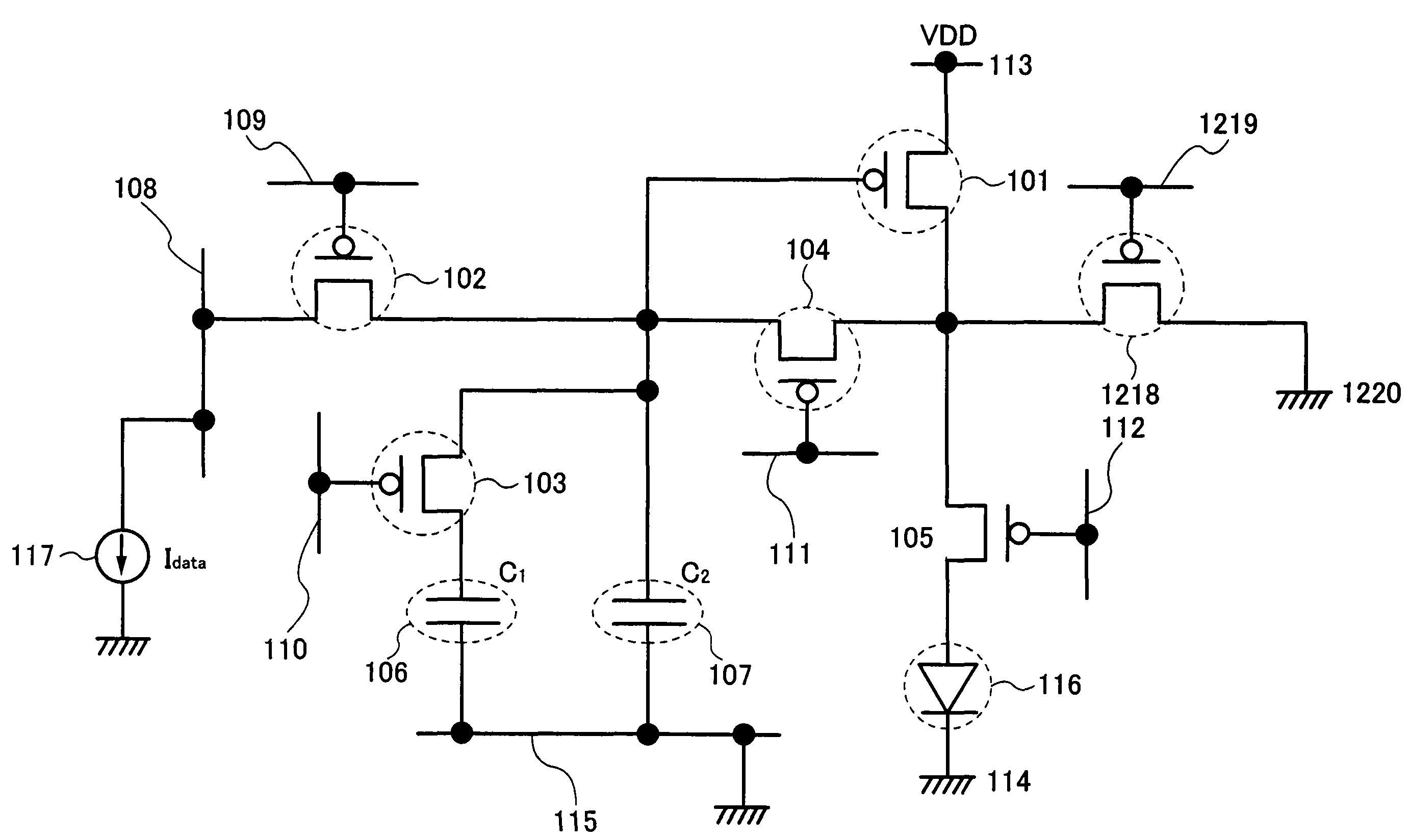
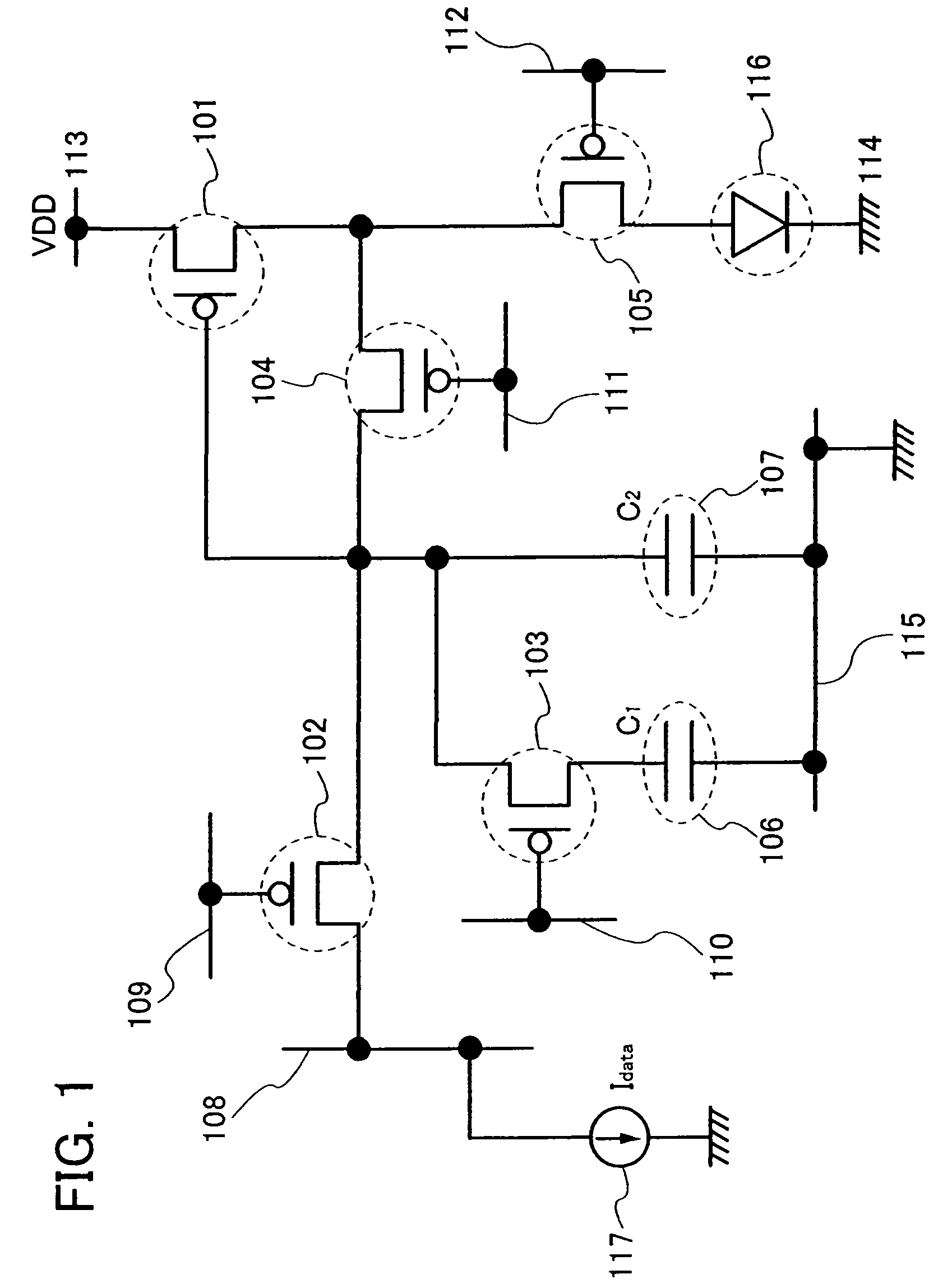
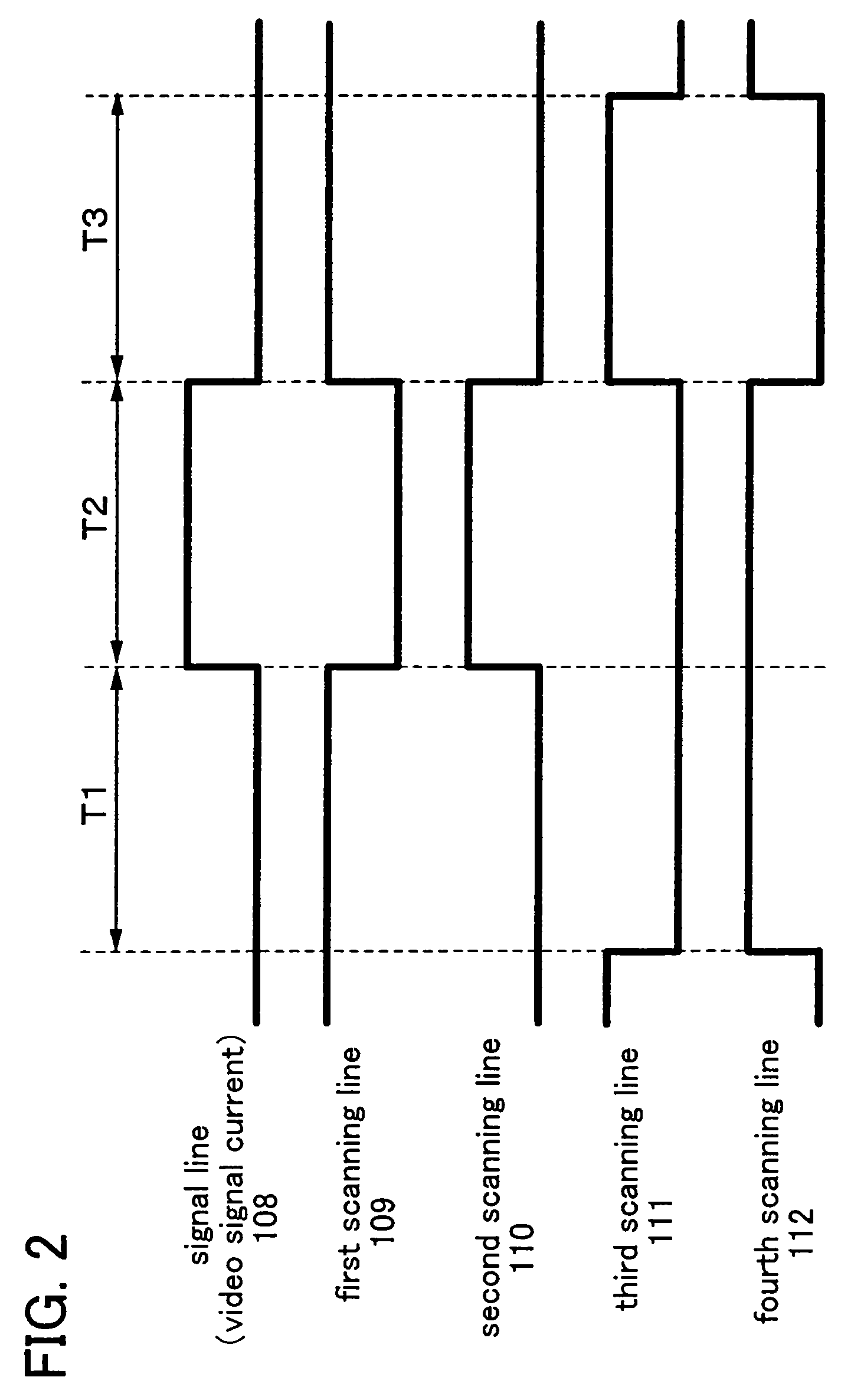
[0135]FIG. 1 is a diagram showing a circuit diagram of a pixel circuit of this embodiment mode. The pixel circuit of this embodiment mode includes first to fifth transistors 101 to 105, first and second storage capacitors 106 and 107, a signal line 108, first to fourth scanning lines 109 to 112, first and second power supply lines 113 and 114, a capacitor line 115, a light-emitting element 116, and a current source circuit 117. Note that the current source circuit 117 is arranged in each signal line (each column).

[0136]Note that, in the pixel circuit shown in FIG. 1, all of the transistors 101 to 105 are p-channel types.

[0137]A gate electrode of the first transistor 101 is connected to a first electrode of the second transistor 102, a first electrode ...

embodiment mode 2

[0226]Although the first and second storage capacitors are connected in parallel in Embodiment Mode 1, the storage capacitors may also be connected in series. Thus, this embodiment mode will explain a case where first and second storage capacitors are connected in series. A basic structure of a pixel circuit in a display device of this embodiment mode will be explained with reference to FIG. 17. Note that the explanation will be given by exemplifying an EL element as a light-emitting element.

[0227]FIG. 17 is a diagram showing a circuit diagram of a pixel circuit of this embodiment mode. The pixel circuit of this embodiment mode includes first to fifth transistors 1701 to 1705, first and second storage capacitors 1706 and 1707, a signal line 1708, first to fourth scanning lines 1709 to 1712, first and second power supply lines 1713 and 1714, a capacitor line 1715, a light-emitting element 1716, and a current source circuit 1717. Note that the current source circuit 1717 is arranged i...

embodiment mode 3

[0315]This embodiment mode will explain a configuration of a signal line driver circuit, a scanning line driver circuit, and the like in a display device, and an operation thereof.

[0316]For example, a display device, as shown in FIG. 1, having a pixel circuit that controls an operation by using the signal line and the first to fourth scanning lines has a configuration as shown in FIG. 62. The display device as shown in FIG. 62 has a pixel portion 6201, first to fourth scanning line driver circuits 6202 to 6205, and a signal line driver circuit 6206.

[0317]First, the signal line driver circuit will be explained. The signal line driver circuit 6206 sequentially outputs a video signal current to the pixel portion 6201 through a signal line 6211. In the pixel portion 6201, an image is displayed by controlling a state of light in accordance with the video signal current.

[0318]FIGS. 63A and 63B each show an example of a configuration of the signal line driver circuit 6206. The signal line ...


PUM


Abstract

One feature of the present invention includes first to third steps of holding a voltage, corresponding to a difference between a voltage applied to a first power supply line and a threshold voltage of a first transistor, between both electrodes of first and second storage capacitors; holding a voltage, corresponding to a difference between a voltage applied to the first power supply line and a gate-source voltage of the first transistor, which is necessary to supply a light-emitting element with a current equivalent to a video signal current inputted into a signal line, between both the electrodes of the second storage capacitor; and applying a voltage based on the voltage held in the first and second storage capacitors in the first and second steps to a gate electrode of the first transistor; therefore, a current is supplied to the light-emitting element through the first transistor.

Description

BACKGROUND OF THE INVENTION[0001]1. Field of the Invention[0002]The present invention relates to a structure of a display device having a transistor. In particular, the present invention relates to a structure of an active matrix display device having a thin film transistor manufactured over an insulator such as glass or plastics. In addition, the present invention relates to an electronic device where a display portion thereof is formed by using such a display device.[0003]2. Description of the Related Art[0004]In recent years, a so-called self-luminous type display device having a pixel that is formed of a light-emitting element such as a light-emitting diode (LED) has been attracting attention. As a light-emitting element used for such a self-luminous type display device, an organic light-emitting diode (OLED) (also referred to as an organic EL element, an electro luminescence: EL element, and the like) has been drawing attention and used for an EL display (for example, an organi...

Claims


Application Information

Patent Timeline
Patent Type & Authority Patents(United States)
IPC IPC(8): G09G3/30H05B44/00
CPCG09G3/3241G09G2300/0465G09G2300/0809G09G2300/0819G09G2300/0852G09G2300/0861H01L27/13G09G2310/0256G09G2310/0262G09G2320/0223G09G2320/043H01L27/12H01L27/1214G09G2310/0251H01L27/127H01L27/1225G09G3/30G09G3/20
Inventor SHISHIDO, HIDEAKI
Owner SEMICON ENERGY LAB CO LTD
Why Eureka
Try Eureka