Active matrix display device, method for driving the same, and electronic device

a technology of active matrix and display device, which is applied in the direction of static indicating device, electroluminescent light source, instruments, etc., can solve the problems of variable luminance of each pixel, and achieve the effect of reducing the number of times signal writing to a pixel, reducing power consumption, and reducing power consumption

Inactive Publication Date: 2014-09-30
SEMICON ENERGY LAB CO LTD
View PDF64 Cites 11 Cited by
  • Summary
  • Abstract
  • Description
  • Claims
  • Application Information

AI Technical Summary

Benefits of technology

[0010]In view of the above, it is an object of the present invention to provide a display device which can reduce the number of times signal writing to a pixel is carried out and power consumption.
[0040]Note that a switch to be described in this specification can be of various types, one example of which is an electric switch, a mechanical switch, or the like. In other words, any switch that can control current flow can be used, and there is no particular limitation. Various switches can be used. For example, the switch may be a transistor, a diode (such as a PN diode, a PIN diode, a Schottky diode, or a diode-connected transistor), or a logic circuit that is a combination thereof. In the case of using a transistor as the switch, the transistor operates as a mere switch. Therefore, the polarity (conductivity type) of the transistor is not particularly limited. However, in the case where lower off-current is desired, it is desirable to use a transistor having a polarity with lower off-current. As the transistor with low off-current, a transistor provided with an LDD region, a transistor having a multigate structure, or the like can be used. In addition, it is desirable to use an n-channel transistor when a transistor to be operated as a switch operates in a state where the potential of a source terminal thereof is close to a lower potential side power source (such as Vss, GND, or 0V), whereas it is desirable to use a p-channel transistor when the transistor operates in a state where the potential of a source terminal thereof is close to a higher potential side power source (such as Vdd). This is because the absolute value of a gate-source voltage can be increased, so that the transistor easily operates as a switch. Note that the switch may be of CMOS type using both an n-channel transistor and a p-channel transistor. If the switch is of CMOS type, it can operate appropriately even when conditions change, for example, a voltage output through the switch (in other words, an input voltage to the switch) is higher or lower than an output voltage.
[0044]Note that the structure of a transistor can be of various types and is not limited to a specific structure. For example, it is possible to use a multigate structure having two or more gates. When using the multigate structure, an off-current can be reduced, the withstand voltage of a transistor can be increased to improve reliability, and variations in characteristics can be suppressed when the transistor operates in the saturation region since a drain-source current does not change much even when a drain-source voltage changes. Alternatively, gate electrodes may be provided above and below a channel. The structure where gate electrodes are provided above and below a channel allows a channel region to be increased; therefore, a current value can be increased and a depletion layer is easily formed to increase the S value. Further, a gate electrode may be provided above a channel or below a channel. A staggered structure or an inverted staggered structure may be adopted. A channel region may be divided into a plurality of regions, and these regions may be connected in parallel or in series. A source electrode or a drain electrode may overlap a channel (or a part of it). The structure where a source electrode or a drain electrode overlaps a channel (or a part of it) prevents charges from being accumulated in a part of the channel, which may cause unstable operation. In addition, an LDD region may be provided. When the LDD region is provided, an off-current can be reduced, the withstand voltage of a transistor can be increased to improve reliability, and variations in characteristics can be suppressed when the transistor operates in the saturation region since a drain-source current does not change much even when a drain-source voltage changes.
[0061]A display device which can reduce the number of times signal writing to a pixel is carried out and power consumption can be provided.
[0062]In other words, the display device of the invention can reduce power consumption by reducing the number of charging and discharging in writing a signal to a pixel.

Problems solved by technology

However, the method to control the light emission intensity in an analog manner is easily affected by variations in characteristics of a thin film transistor (hereinafter also referred to as a TFT) of each pixel, which causes variations also in luminance of each pixel.

Method used


Image

  • Active matrix display device, method for driving the same, and electronic device
  • Active matrix display device, method for driving the same, and electronic device
  • Active matrix display device, method for driving the same, and electronic device

Examples


embodiment mode 1

[0195]In this embodiment mode, detailed explanation is made on a display device and operation thereof in the case of applying the present invention to a time gray scale method.

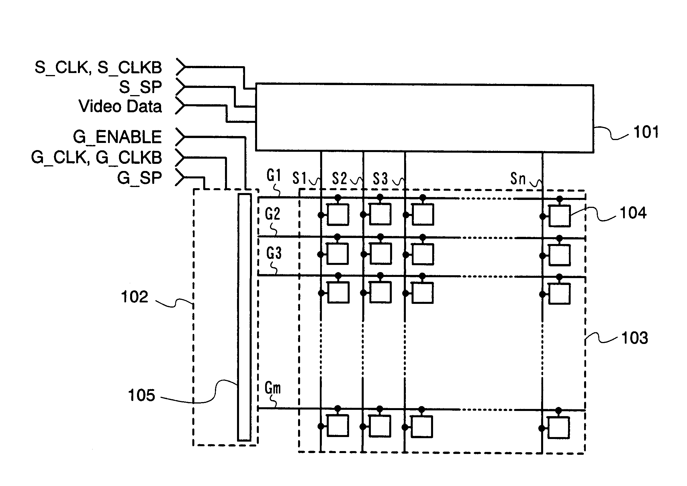
[0196]A display device shown in FIG. 1 includes a signal line driver circuit 101, a scan line driver circuit 102, and a pixel portion 103. In addition, a plurality of pixels 104 is arranged in matrix in the pixel portion 103 relative to signal lines S1 to Sn extended from the signal line driver circuit 101 in a column direction and scan lines G1 to Gm extended from the scan line driver circuit 102 in a row direction. In addition, the scan line driver circuit 102 includes an output control circuit 105.

[0197]Signals such as a clock signal (G_CLK), an inverted clock signal (G_CLKB), a start pulse signal (G_SP), and an output control signal (G_ENABLE) are input to the scan line driver circuit 102.

[0198]The clock signal (G_CLK) is a signal alternating between H (High) and L (Low) at regular intervals, and the inver...

embodiment mode 2

[0221]In this embodiment mode, explanation is made on a line sequential display device of the present invention and operation thereof.

[0222]FIG. 3 shows a schematic diagram of a line sequential display device. A signal line driver circuit 301 corresponds to the signal line driver circuit 101 of the display device in FIG. 1. Other common components are denoted by reference numerals in common with those in FIG. 1, and explanation thereof is omitted.

[0223]The signal line driver circuit 301 includes a pulse output circuit 302, a first latch circuit 303, a second latch circuit 304, and an output control circuit 305.

[0224]A clock signal (S_CLK), an inverted clock signal (S_CLKB), a start pulse signal (S_SP), and the like are input to the pulse output circuit 302. Then, a sampling pulse is output in accordance with the timing of these signals.

[0225]A sampling pulse output from the pulse output circuit 302 is input to the first latch circuit 303. A video signal (Video Data) is input to the ...

embodiment mode 3

[0279]Subsequently, FIG. 4 shows a schematic diagram of a dot sequential display device. A signal line driver circuit 401 corresponds to the signal line driver circuit 101 of the display device in FIG. 1. Other common components are denoted by reference numerals in common with those in FIG. 1, and explanation thereof is omitted.

[0280]The signal line driver circuit 401 includes a pulse output circuit 402, a switch group 403, and an output control circuit 404.

[0281]A clock signal (S_CLK), an inverted clock signal (S_CLKB), a start pulse signal (S_SP), and the like are input to the pulse output circuit 402. Then, a sampling pulse is output in accordance with the timing of these signals.

[0282]A sampling pulse output from the pulse output circuit 402 is input to the switch group 403. A video signal (Video Data) is input to respective one of terminals of switches in the switch group 403, and the respective other terminal is connected to respective one of signal lines S1 to Sn through the ...


PUM


Abstract

An object of the invention is to provide a display device which can reduce the number of times signal writing to a pixel is carried out and power consumption. A display device which can reduce the number of times signal writing to a pixel is carried out and power consumption can be provided. According to an active matrix display device of the invention, in the case a signal to be written to a pixel row is identical with a signal stored in the pixel row, the scan line driver circuit does not output a selecting pulse to a scan line corresponding to the pixel row, and the signal line driver circuit makes the signal lines in a floating state or keeps without changing the state of the signal line from the previous state.

Description

BACKGROUND OF THE INVENTION[0001]1. Field of the Invention[0002]The present invention relates to a semiconductor device having a function to control a current supplied to a load by a transistor, and to a display device including a pixel formed with a current-drive display element of which luminance is changed by a signal, a pixel formed with a voltage-drive display element of which luminance is changed by a voltage, and a signal line driver circuit and a scan line driver circuit thereof. The present invention also relates to a method for driving the same. The present invention further relates to an electronic device including the display device in a display portion.[0003]2. Description of the Related Art[0004]In recent years, a so-called self-luminous display device in which a pixel is formed using a display element such as a light emitting diode (LED) has attracted attention. As a display element used for such a self-luminous display device, an organic light emitting diode (also re...

Claims


Application Information

Patent Timeline
Patent Type & Authority Patents(United States)
IPC IPC(8): G09G3/34G09G3/20G09G3/32G09G5/395G09G5/399H05B44/00
CPCG09G3/3233G09G3/2022G09G5/395G09G3/3258G09G3/3266G09G2320/10G09G2320/103G09G2300/0842G09G2300/0408G09G2300/0861G09G3/3275G09G5/399G09G2330/021G09G2310/0221G09G2340/16G09G3/30G09G3/20G09G3/32H05B33/00
Inventor KIMURA, HAJIME
Owner SEMICON ENERGY LAB CO LTD
Why Eureka
Try Eureka