

Touch panel and manufacturing method thereof
- Summary
- Abstract
- Description
- Claims
- Application Information
AI Technical Summary
Benefits of technology
Problems solved by technology
Method used
Image

Examples
Embodiment Construction
[0020]The aforementioned illustrations and following detailed descriptions are exemplary for the purpose of further explaining the scope of the present invention. Other objectives and advantages related to the present invention will be illustrated in the subsequent descriptions and appended drawings.
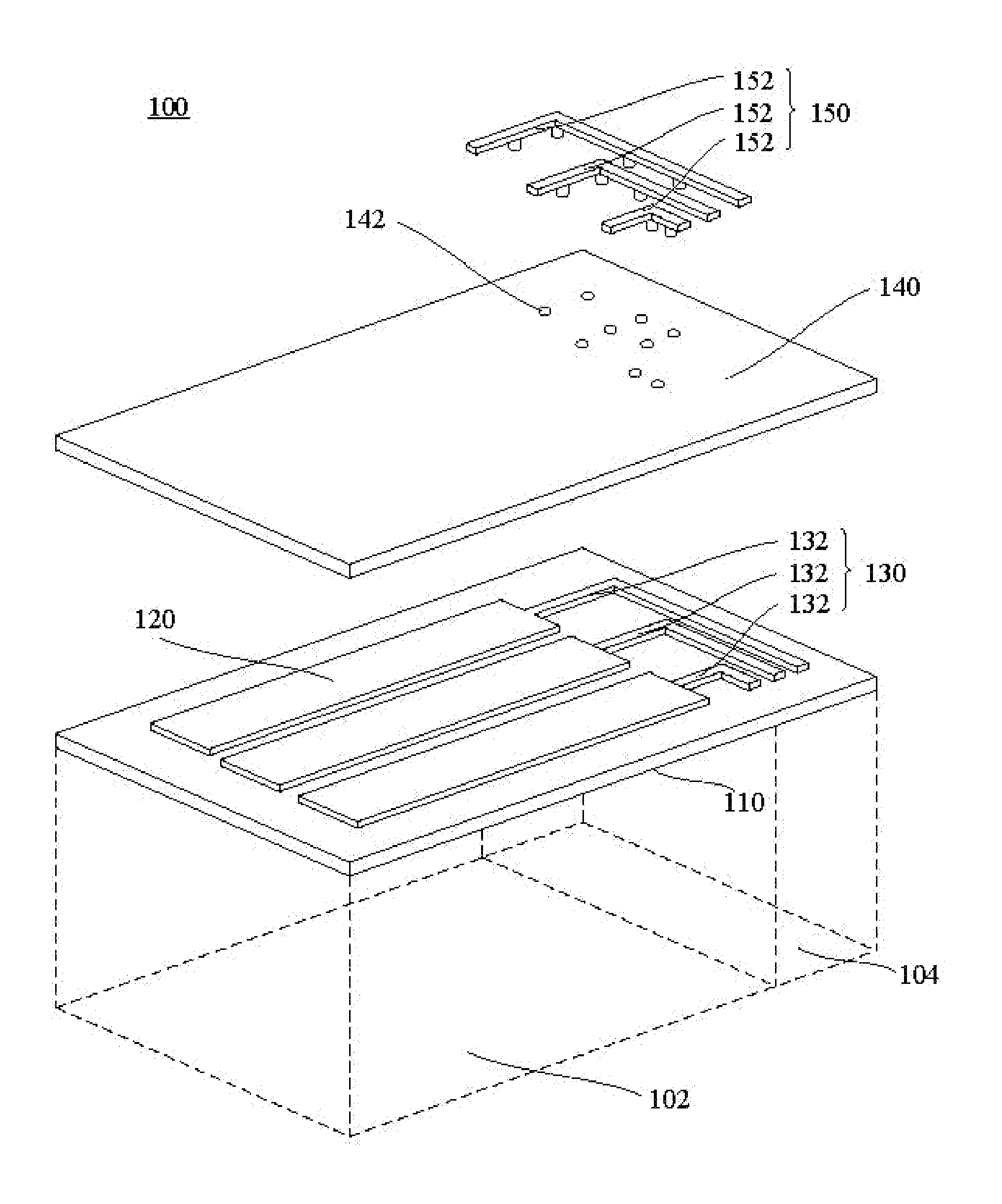
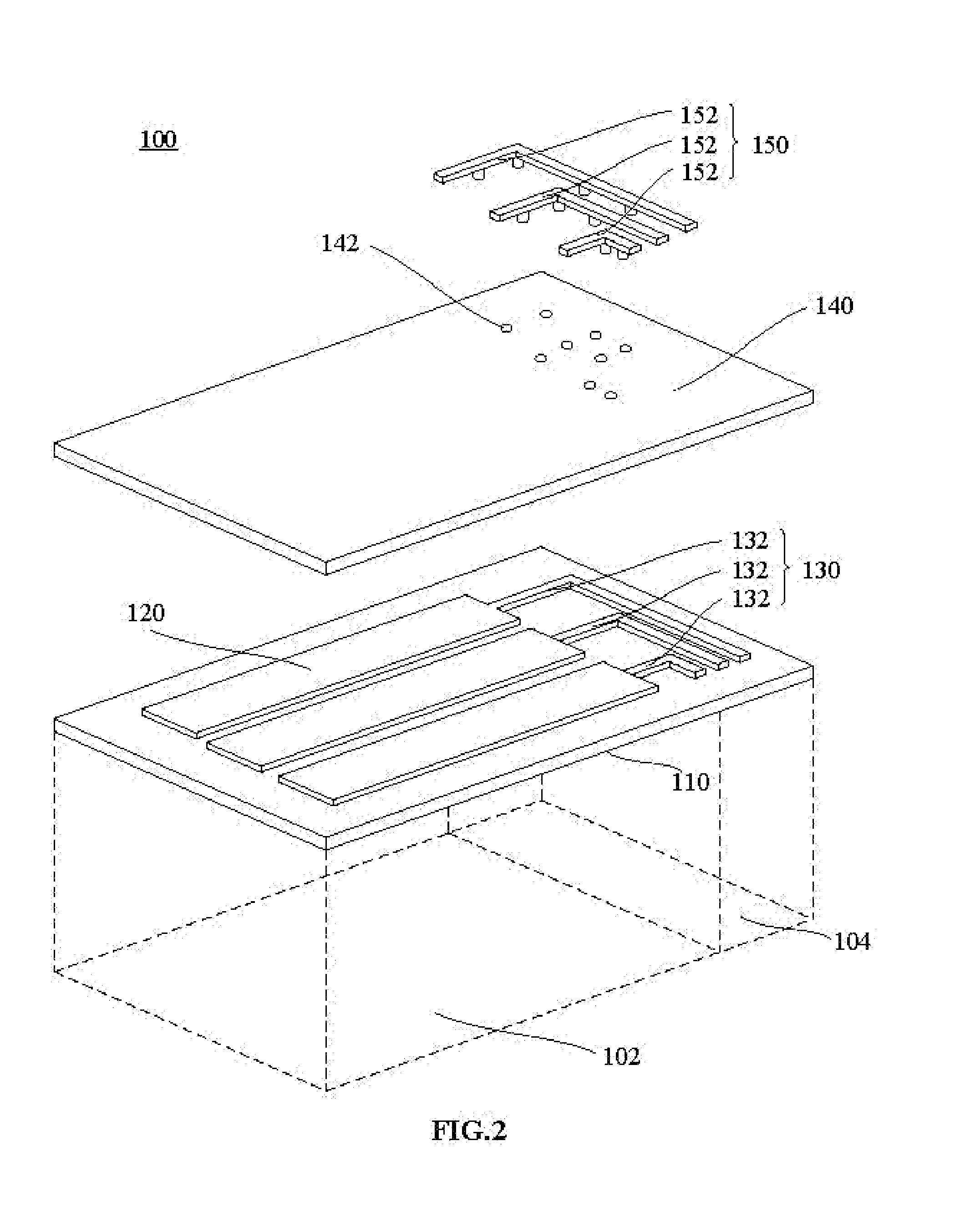
[0021]FIG. 2 is an exploded view of a touch panel according to a first embodiment. The touch panel 100 is partitioned into a sensing region 102 and a circuit region 104 positioned along the edge of the sensing region 102. The touch panel 100 includes an electrode layer 120, a first wire layer 130, an insulating layer 140 and a second wire layer 150. The position and amount of the circuit region 104 can be adjusted according to the particular structure of the electrode layer 120 and the amount of first wires 132 included in a first wire layer 130. For example, the circuit region 104 can be positioned at one side or more than one side of the electrode layer 120. The electrode layer 120 is ...
PUM
| Property | Measurement | Unit |
|---|---|---|
| Transparency | aaaaa | aaaaa |
Abstract
Description
Claims
Application Information