

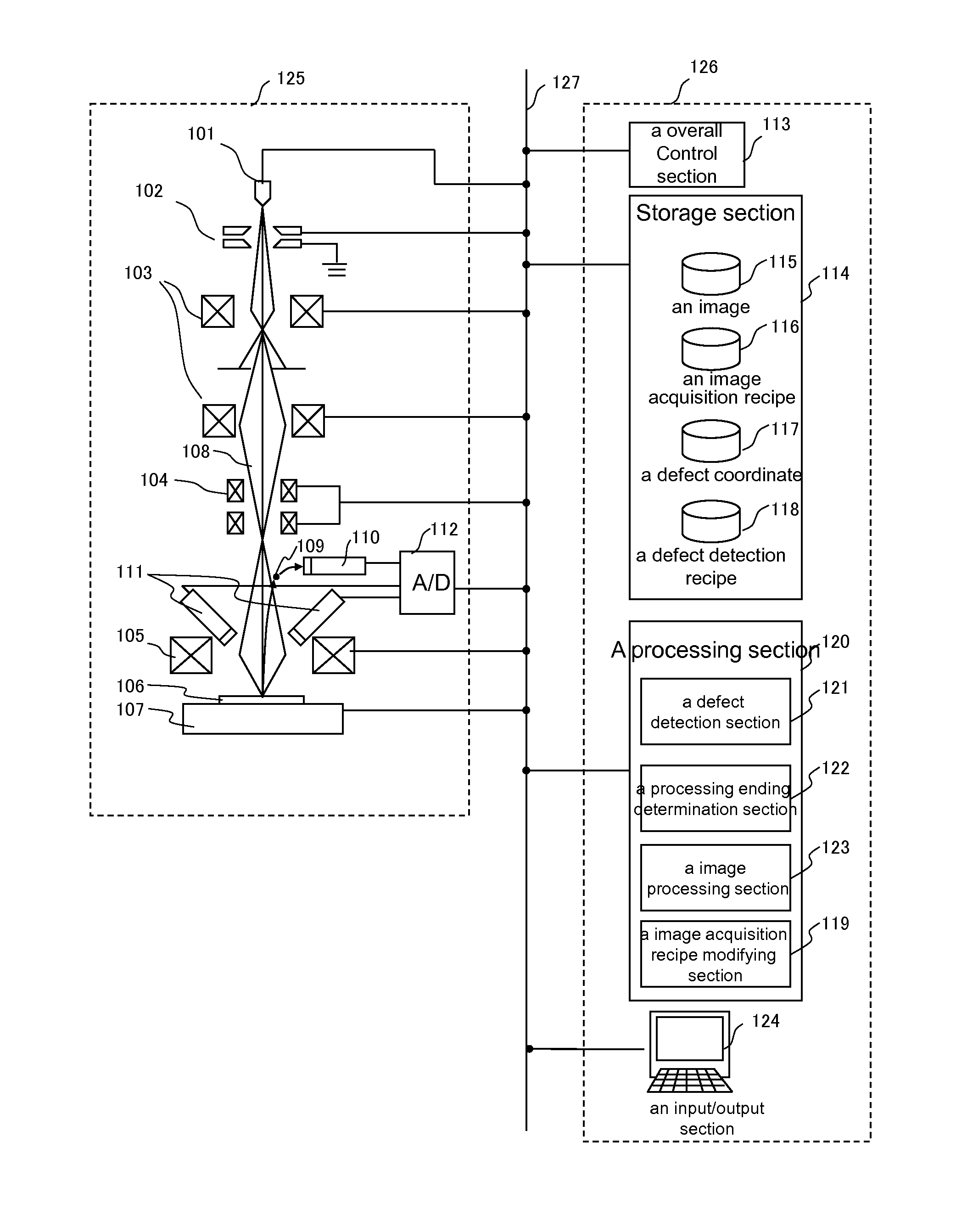
Method and Apparatus for Reviewing Defect
a defect inspection and defect technology, applied in the field of defect inspection methods and defect inspection apparatuses, can solve the problems of increased defect inspection time, difficulty in exact detail discrimination between defect type and actual defect type, and increased number of defects to be reviewed per wafer. , to achieve the effect of shortening the time for defect image obtaining
- Summary
- Abstract
- Description
- Claims
- Application Information
AI Technical Summary
Benefits of technology
Problems solved by technology
Method used
Image

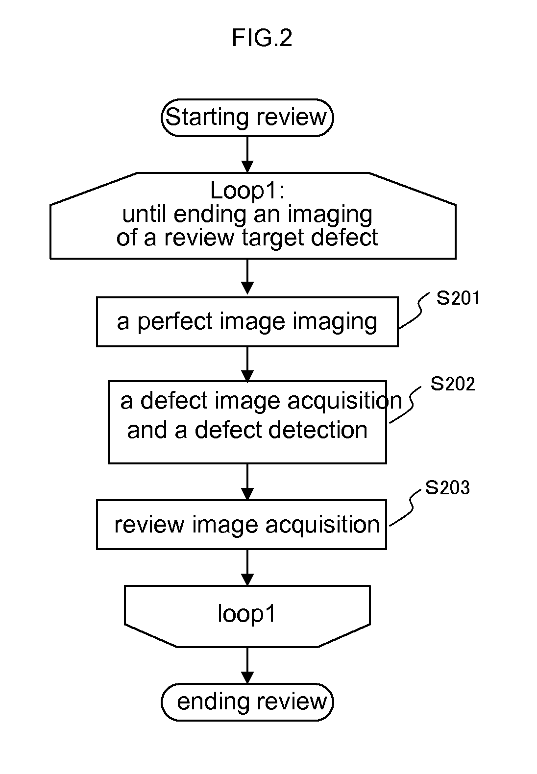
Examples
first embodiment
(Frame Addition Amount)
[0185]Hereinafter, in case that the image acquisition conditions, which frame addition amounts are different, is registered in the image acquisition recipe will be described.
[0186]In general, if the frame addition amount increases, S / N of obtained image also increases, but the image obtaining time also increases.
[0187]In particular, in case of large defects, it is possible to obtain a high defect detection accuracy even though the images are imaged by some low S / N imaging obtaining condition .
[0188]It is possible to conclude the image acquisition and the defect detection at short times.
[0189]A method of proceeding of S301 will be described in case that the image acquisition conditions' frame addition amounts are different.
[0190]Hereinafter, it will be described in case that the conditions (N) stored frame addition amount of consecutive and different values is registered in the image acquisition recipe storage section 116.
[0191]In this case, only the frame addi...
second embodiment
(Image Size (Pixel Size))
[0230]Then, in case that the image acquisition recipe stores the image acquisition conditions (however imaging field of view is assumed to constant for purpose of illustration) which image sizes (pixel size) are different will be described.
[0231]An image size, a pixel size and a imaging field of view have a relation each other , in case that the imaging field of view is constant, if the image size increases, the image of smaller pixel size (that is high-resolution) could be obtained but the image acquisition time increases.
[0232]The image acquisition recipe registers the conditions storing three values which three values are (1) small, (2) middle, (3) large of image size (pixel sizes are (1) large, (2) middle, (3) small).
[0233]FIG. 6 is obtaining image examples and defect detection accuracy of these images illustrating the first embodiment of in case that the image obtaining is done about defects which largeness are different using the image obtaining condit...
third embodiment
(Image Size (Imaging Field of View))
[0249]Then, in case that the image acquisition conditions which differ the image size (imaging field of view) are registered in the image acquisition recipe (however pixel size is assumed to constant for purpose of illustration).
[0250]An image size, a pixel size and a imaging field of view have a relation each other , in case that the imaging field of view is constant, if the image size increases, the image of larger field of view (that is large area) could be obtained but the image acquisition time increases.
[0251]The image acquisition recipe registers the image acquisition conditions storing three values which three values are (1) small, (2) middle, (3) large of image size (fields of view are (1) small, (2) middle, (3) large).
[0252]FIG. 7 is obtaining image examples and defect detection accuracy of these images illustrating the first embodiment of in case that the image obtaining is done about defects coordinates accuracies are different using t...
PUM
 Abstract
Description
Claims
Application Information