Rectifying device, electronic circuit using the same, and method of manufacturing rectifying device

a technology of rectifying device and electronic circuit, which is applied in the direction of semiconductor devices, material nanotechnology, electrical devices, etc., can solve the problems of not being desirable from the viewpoint of load to the environment, the structure of a device using silicon that is currently going mainstream can only meet the requirements in a limited range, and the number of reported rectifying devices using carbon nanotubes is not very large, so as to achieve the effect of using the properties of carbon nanotube structur

Inactive Publication Date: 2014-08-14
FUJIFILM BUSINESS INNOVATION CORP
View PDF0 Cites 4 Cited by
  • Summary
  • Abstract
  • Description
  • Claims
  • Application Information

AI Technical Summary

Benefits of technology

[0020]The carrier transporter in the present invention is preferably composed of multiple carbon nanotubes. When the carrier transporter is composed of one carbon nanotube, the maximum current that can flow is small. However, the use of multiple carbon nanotubes can increase the maximum current. In addition, a carrier transporter composed of multiple carbon nanotubes is superior in safety to that composed of one carbon nanotube because an electrical network in the carrier transporter is surely formed.
[0110]Examples of the functional group particularly preferable for use in dehydration condensation include —COOH. Introduction of a carboxyl group into carbon nanotubes is relatively easy, and the resultant substance (carbon nanotube carboxylic acid) has high reactivity. Therefore, functional groups for forming a network structure can be easily introduced into multiple sites of one carbon nanotube. Moreover, the functional group is suitable for formation of a carbon nanotube structure because the functional group is easily subjected to dehydration condensation.

Problems solved by technology

However, at present, the structure of a device using silicon that is currently going mainstream can satisfy the requirements only in a limited range owing to the limitations on silicon as a material.
The use of a semiconductor material such as gallium arsenide is not desirable from the viewpoint of load to the environment.
However, the number of reported rectifying devices using carbon nanotubes is not very large, and the number of production examples of devices each of which has a controlled rectifying direction is smaller.
However, the existing rectifying devices using carbon nanotubes as carrier transporters are not suitable for practical use because their rectifying directions cannot be controlled.

Method used


Image

  • Rectifying device, electronic circuit using the same, and method of manufacturing rectifying device
  • Rectifying device, electronic circuit using the same, and method of manufacturing rectifying device
  • Rectifying device, electronic circuit using the same, and method of manufacturing rectifying device

Examples


example 1

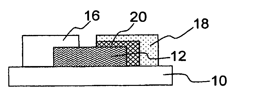
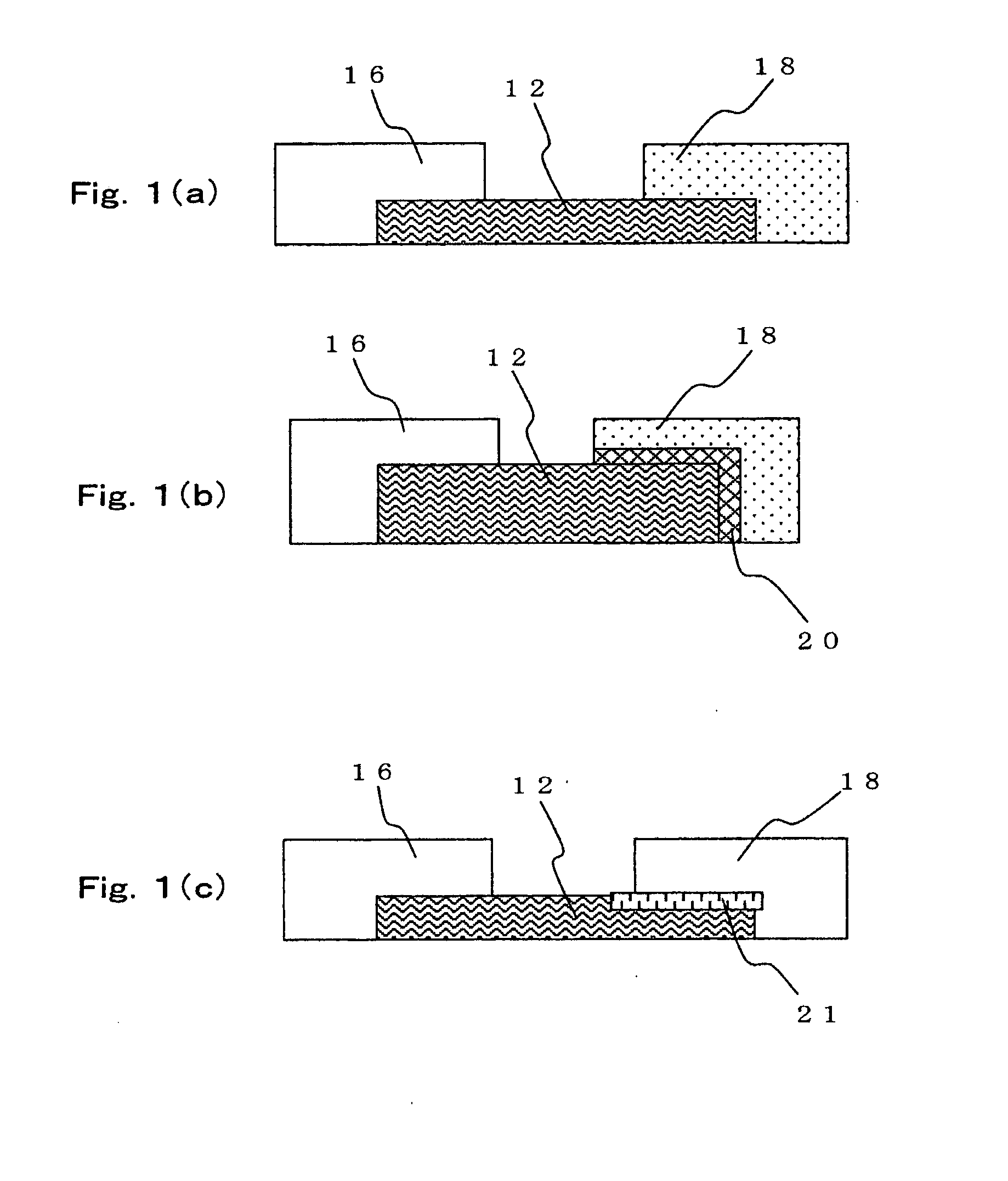
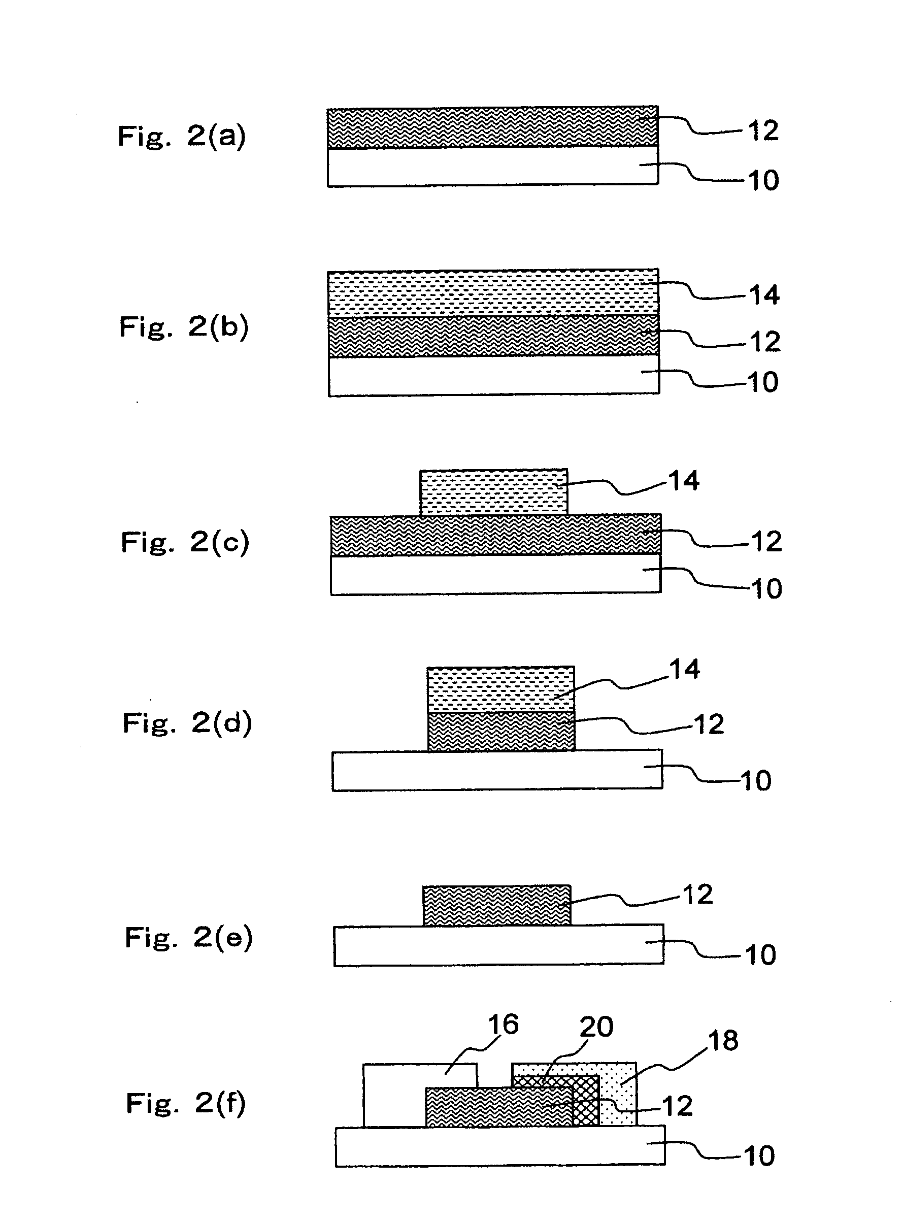
[0349]In this example, a rectifying device using a glycerin-cross-linked film of single-wall carbon nanotubes having semiconductor properties as a carrier transporter was prepared according to the flow of the method of manufacturing a rectifying device shown in FIG. 2. Titanium and aluminum were used as electrode materials to form electrodes. Aluminum was naturally oxidized to form an oxide film at an electrode-carbon nanotube structure interface. Reference numerals shown in FIG. 2 may be used in the description of this example.

(A) Supplying Step

(A-1) Preparation of Cross-Linking Solution (Addition Step)

(i) Purification of Single-Wall Carbon Nanotube

[0350]Single-wall carbon nanotube powder (purity: 40%, available from Sigma-Aldrich Co.) was sieved (pore size of 125 μm) in advance to remove a coarse aggregate. 30 mg of the resultant (having an average diameter of 1.5 nm and an average length of 2 μm) were heated at 450° C. for 15 minutes by means of a muffle furnace to remove a carbo...

example 2

[0379]A device using a cross-linked film of multi-wall carbon nanotubes as a carrier transporter was prepared according to the same method as that described in Example 1. An aluminum natural oxide film was formed as an oxide film at an interface between an aluminum electrode and a carbon nanotube structure in the same manner as in Example 1. Titanium was used as a material for the other electrode. A method of forming a coat is shown below. The other steps were the same as those of Example 1.

(A) Supplying Step

(A-1) Preparation of Cross-Linking Solution (Addition Step)

(i) Addition of Carboxyl Group . . . Synthesis of Carbon Nanotube Carboxylic Acid

[0380]30 mg of multi-wall carbon nanotube powder (purity: 90%, average diameter: 30 nm, average length: 3 μm, available from Science Laboratories, Inc.) were added to 20 ml of concentrated nitric acid (60 mass % aqueous solution, available from Kanto Kagaku) for reflux at 120° C. for 20 hours, to synthesize a carbon nanotube carboxylic acid....

example 3

[0385]In this example, as shown in FIG. 6, a rectifying device having a sandwich structure in which a carrier transporter was sandwiched on a substrate was manufactured. FIG. 6 is a sectional diagram of the rectifying device of this example.

[0386]An aluminum electrode 3 serving as a main electrode was formed in advance on a silicon wafer (not shown) serving as a substrate. An alumina (Al2O3) layer 4 for forming a barrier was laminated by means of deposition on the aluminum electrode 3.

[0387]Next, in the same manner as in Example 1, a single-wall carbon nanotube structure 1 serving as a carrier transporting layer was formed. Furthermore, titanium / gold was deposited as an upper electrode 2 to manufacture a rectifying device. The deposited alumina had a thickness of about 70 nm.

[Evaluation Test (Measurement of Current-Voltage Characteristics)]

[0388]Direct current-voltage characteristics of the devices of Examples 1 to 3 were measured.

[0389]The measurement was performed according to the...


PUM


Abstract

To provide a rectifying device equipped with a carrier transporter excellent in high frequency responsiveness and heat resistance, an electronic circuit using the same, and a method of manufacturing the rectifying device. The rectifying device includes a pair of electrodes, and a carrier transporter arranged between the pair of electrodes and composed of one or multiple carbon nanotubes. In order that a first interface between one electrode of the pair of electrodes and the carrier transporter and a second interface between the other electrode of the pair of electrodes and the carrier transporter may have different barrier levels, connection configuration of them are made different.

Description

RELATED APPLICATION[0001]This application is a Divisional application of U.S. patent application Ser. No. 10 / 580,436, filed May 24, 2006.TECHNICAL FIELD[0002]The present invention relates to a rectifying device using a carbon nanotube structure as a carrier transporter, an electronic circuit using the same, and a method of manufacturing a rectifying device.BACKGROUND ART[0003]Carbon nanotubes (CNTs), with their unique shapes and characteristics, may find various applications. A carbon nanotube has a tubular shape of one-dimensional nature which is obtained by rolling one or more graphene sheets composed of six-membered rings of carbon atoms into a tube. A carbon nanotube formed from one graphene sheet is called a single-wall carbon nanotube (SWNT) while a carbon nanotube formed from multiple graphene sheets is called a multi-wall carbon nanotube (MWNT). SWNTs are about 1 nm in diameter whereas multi-wall carbon nanotubes are several tens nm in diameter, and both are far thinner than...

Claims


Application Information

Patent Timeline
Patent Type & Authority Applications(United States)
IPC IPC(8): H01L51/00H01L51/10H01L29/872H01L51/30
CPCH01L51/0048H01L51/0021Y10S977/742B82Y30/00H01L51/102B82Y10/00H10K85/225H10K85/221H10K10/23H10K10/82H10K10/00H01L29/872H10K71/60
Inventor OKADA, SHINSUKEHIRAKATA, MASAKIMANABE, CHIKARAANAZAWA, KAZUNORISHIGEMATSU, TAISHIWATANABE, MIHOKISHI, KENTAROISOZAKI, TAKASHIOOMA, SHIGEKIWATANABE, HIROYUKI
Owner FUJIFILM BUSINESS INNOVATION CORP
Why Eureka
Try Eureka