Light emitting device mount, light emitting apparatus including the same, and leadframe

a technology of light emitting devices and mounting brackets, which is applied in the direction of solid-state devices, electrical apparatus construction details, basic electric elements, etc., can solve the problem of sealing resin material leaking to the bottom surface, and achieve the effect of suppressing the leakage of sealing resin material or the entry of solder flux

Active Publication Date: 2014-09-18
NICHIA CORP
View PDF2 Cites 23 Cited by
  • Summary
  • Abstract
  • Description
  • Claims
  • Application Information

AI Technical Summary

Benefits of technology

[0011]According to the present invention, it is possible to keep the strength of the peripheral edge parts of the leadfr

Problems solved by technology

However, in the semiconductor apparatus disclosed in JP 2012-039,109, the material of the sealing resin member may leak to the bo

Method used


Image

  • Light emitting device mount, light emitting apparatus including the same, and leadframe
  • Light emitting device mount, light emitting apparatus including the same, and leadframe
  • Light emitting device mount, light emitting apparatus including the same, and leadframe

Examples


first embodiment

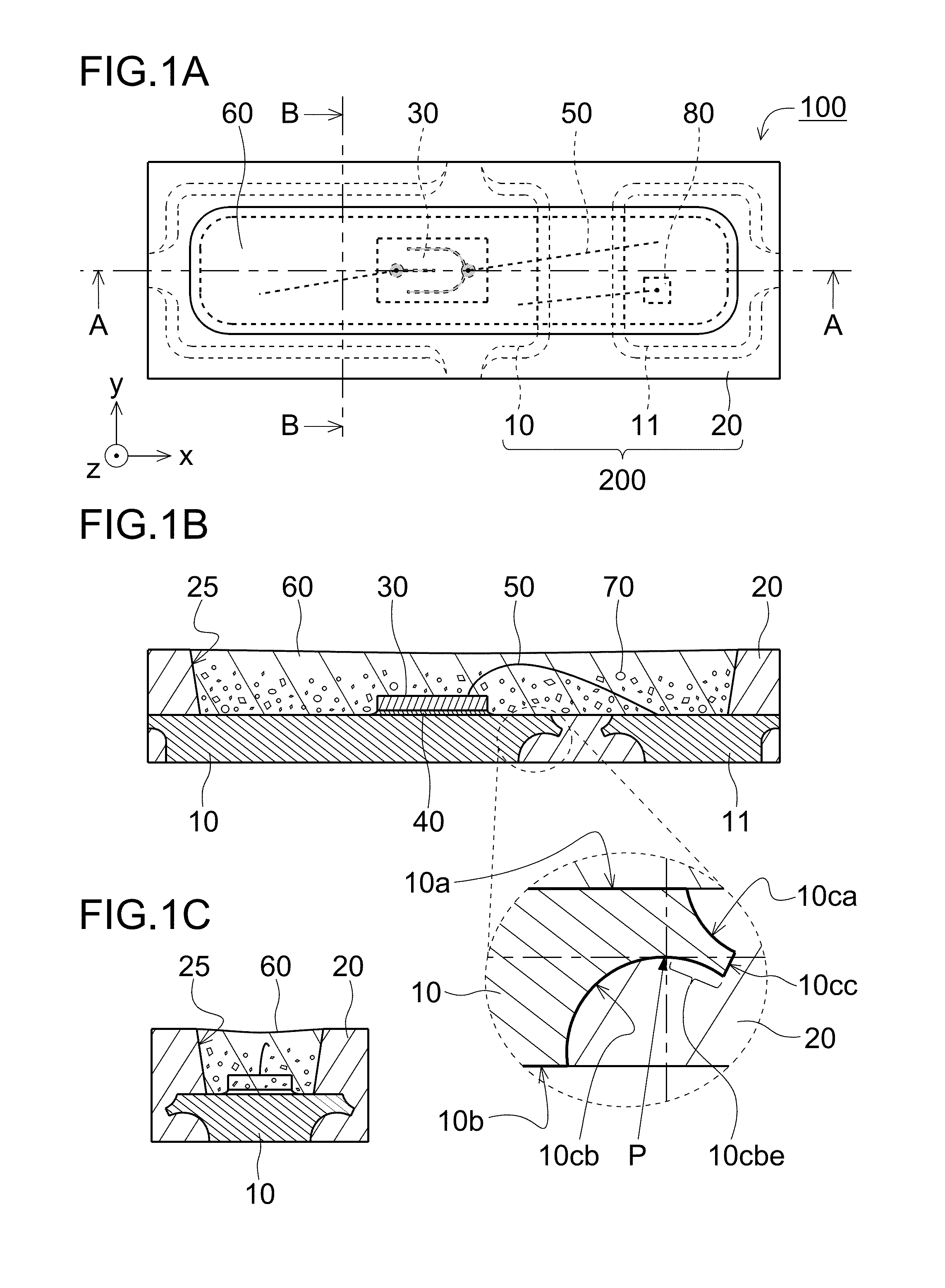
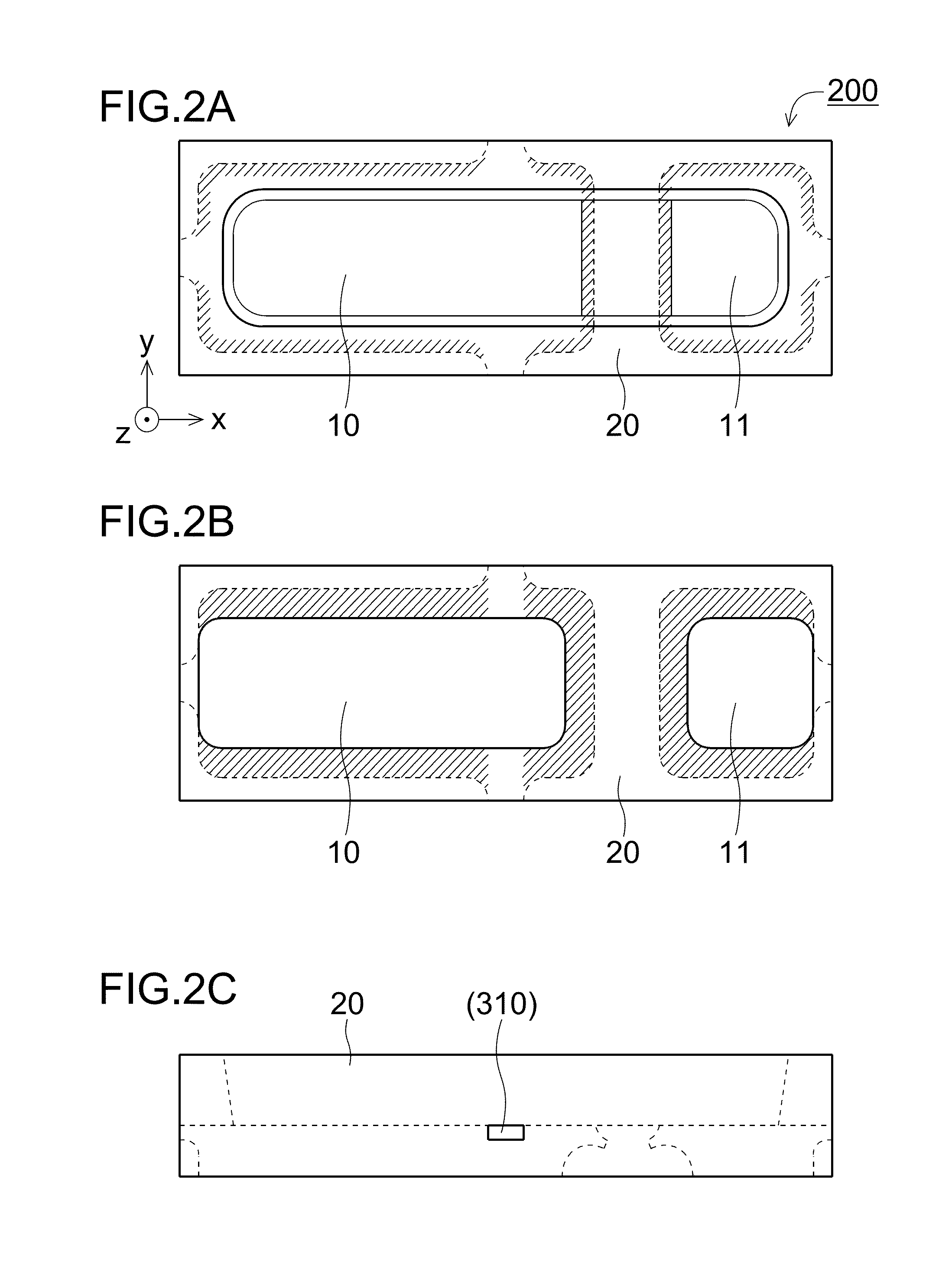
[0024]FIG. 1A is a schematic plan view schematically showing a light emitting apparatus 100 according to a first embodiment of the present invention. FIG. 1B is a schematic cross-sectional view of the light emitting apparatus 100 taken along the line A-A shown in FIG. 1A. FIG. 1C is a schematic cross-sectional view of the light emitting apparatus 100 taken along the line B-B shown in FIG. 1A. FIG. 2A is a schematic plan view of a light emitting device mount 200 according to the first embodiment of the present invention. FIG. 2B is a schematic bottom view of the light emitting device mount 200. FIG. 2C is a schematic side view of the light emitting device mount 200.

[0025]As shown in FIGS. 1A to 1C, the light emitting apparatus 100 according to the first embodiment includes the light emitting device mount 200, and a light emitting device 30 that is mounted on the light emitting device mount 200. Specifically, the light emitting apparatus 100 is mainly constructed of the light emitting...

second embodiment

[0043]FIG. 4 is an enlarged schematic cross-sectional view showing a part of a light emitting apparatus according to a second embodiment of the present invention. The construction of the light emitting apparatus according to this embodiment shown in FIG. 4 is substantially the same as the light emitting apparatus according to the first embodiment except for the arrangement of the main surfaces of the first and second recessed surface areas in the lead terminal, and the relationship between the lead terminal and the resin portion. The description of the same construction of the light emitting apparatus according to this embodiment is omitted for ease of explanation.

[0044]The end surfaces of the lead terminal in the light emitting apparatus according to this embodiment shown in FIG. 4 also include the first and second recessed surface areas 10ca and 10cb that extend from the first and second main surfaces 10a and 10b, respectively. The second recessed surface area 10cb includes a clos...

example 1

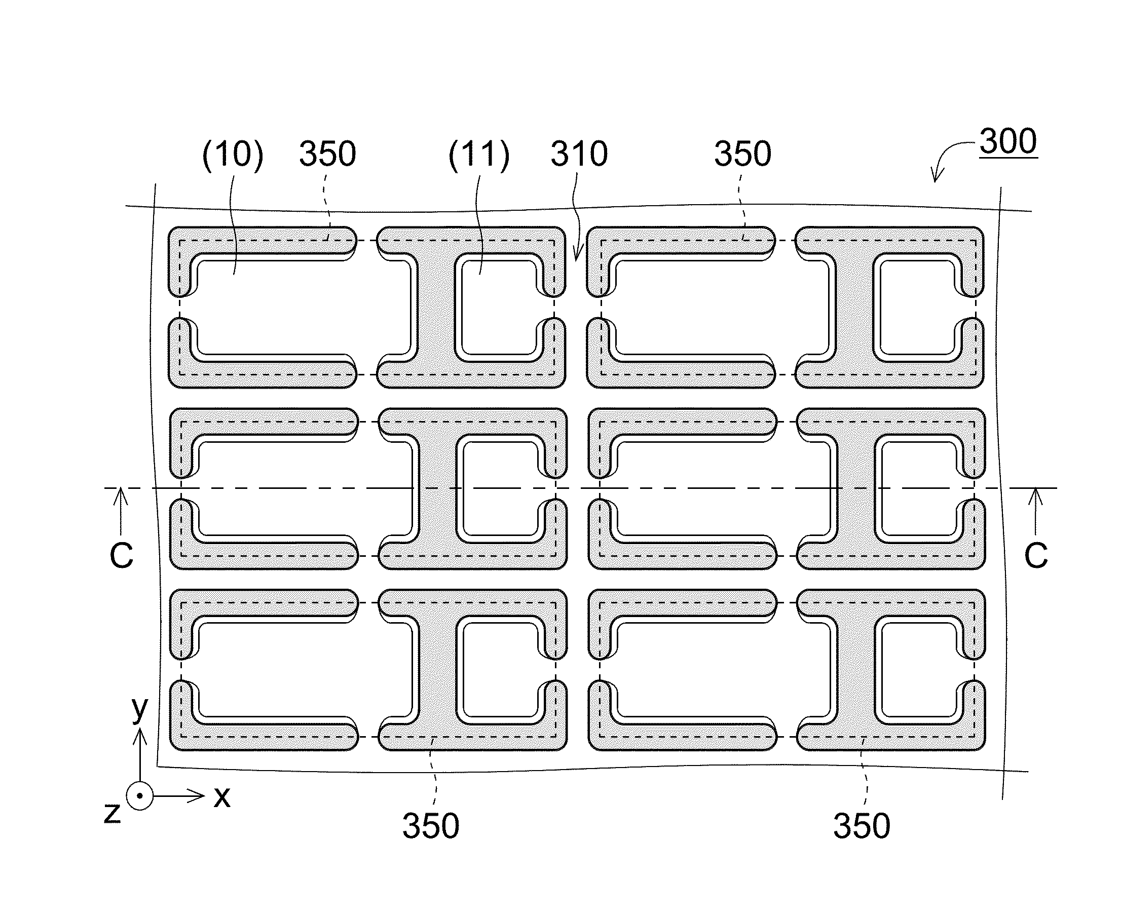
[0065]The light emitting apparatus according to an example 1 is a SMD type LED that emits light upward and has a similar structure to the light emitting apparatus 100 according to the embodiment shown in FIGS. 1A to 1C. The light emitting apparatus has an approximately rectangular box exterior shape. The light emitting apparatus includes the light emitting device mount as package for light emitting apparatus. The light emitting device mount has a length of 3.0 mm, a width of 1.0 mm, and a thickness of 0.52 mm. The resin portion is integrally formed with the first and second lead terminals as positive and negative terminals. The leadframe is first placed into a die. The leadframe includes a plurality of lead terminal sets (pairs of lead terminals) that are arranged in matrix and are held by the hanger leads. Subsequently, a resin material with fluidity is injected into the die. After the resin material is solidified, the leadframe with the resin material is removed from the die. The ...


PUM


Abstract

A mount includes a terminal, and a resin portion. The terminal includes a first surface, a second surface, and an end surface having first and second recessed areas that are extend from the first and second surfaces, respectively. The resin portion is integrally formed with the terminal, and at least partially covers the end surface so that the first and second surfaces are at least partially exposed. The resin portion forms a recessed part to accommodate the light emitting device. The second recessed area includes a closest point that is positioned closest to the first surface, and an extension part that extends outward of the closest point and toward the second surface side. The extension part is formed at least on opposing end surfaces of the pair of positive and negative lead terminal. The first recessed area is arranged on the exterior side relative to the closest point.

Description

BACKGROUND OF THE INVENTION[0001]1. Field of the Invention[0002]The present invention relates to a light emitting device mount, a light emitting apparatus including the mount, and a leadframe.[0003]2. Description of the Related Art[0004]See Japanese Patent Laid-Open Publication No. 2012-039,109.[0005]It discloses a semiconductor apparatus including a leadframe that is produced by subjecting both the top and bottom surfaces of a metal base plate to etching, an LED (light emitting diode) device that is arranged on the leadframe, an external resin portion that has a recessed part for enclosing the LED device and is integrally formed with the leadframe, and a sealing resin member with which the recessed part is filled.[0006]However, in the semiconductor apparatus disclosed in JP 2012-039,109, the material of the sealing resin member may leak to the bottom surface, or solder flux may enter the recessed part through a small gap between the leadframe and the external resin portion.[0007]Th...

Claims


Application Information

Patent Timeline
IPC IPC(8): H01L23/495H01L33/48
CPCH01L33/483H01L23/495H01L24/45H01L24/97H01L33/486H01L33/62H01L23/49562H01L23/49548H01L24/29H01L24/48H01L24/32H01L24/73H01L2224/32245H01L2224/45169H01L2224/45147H01L2224/45144H01L2224/45139H01L2224/45124H01L2224/2929H01L2224/29339H01L2224/29301H01L2224/29344H01L2224/29364H01L2224/2919H01L2224/45565H01L2224/45639H01L2224/48091H01L2224/48247H01L2224/73265H01L2924/0781H01L2924/07802H01L2924/12041H01L2924/0132H01L2933/0033H01L2933/0066H01L2924/18301H01L2924/00014H01L2924/0665H01L2924/0715H01L2924/07025H01L2924/095H01L2924/0105H01L2924/01083H01L2924/01047H01L2924/01079H01L2924/00012H01L2924/00H01L2224/45015H01L2924/181H01L2924/12035H01L2924/12042H01L2224/45173H01L2224/45184H01L2224/45644H01L2224/45647H01L2224/45655H01L2224/45657H01L2224/4566H01L2224/45673H01L2224/4568H01L2224/45684H01L2224/48257H01L2224/97H01L2924/00011H01L2924/20752H01L2924/01049H01L33/54H01L2224/45624H01L23/49517H01L23/49541H01L33/52
Inventor YAMASHITA, RYOHEIYOSHIMOTO, RYOICHI
Owner NICHIA CORP
Why Eureka
Try Eureka